 ALLPCB


If you're diving into rigid-flex PCB design, you're likely looking for clear guidelines to ensure reliability and performance, especially in critical areas like plated through-holes and bending zones. In this comprehensive guide, we'll walk you through the essentials of rigid-flex PCB design, focusing on best practices for plated through-holes and bending areas to help you create durable and efficient boards. Whether you're a seasoned engineer or new to this technology, you'll find actionable tips and detailed insights to optimize your next project.
What is Rigid-Flex PCB Design?
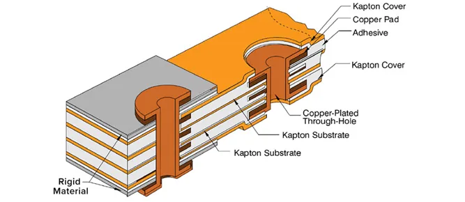
Rigid-flex PCBs combine the benefits of rigid and flexible circuit boards into a single design. This hybrid approach allows for greater design freedom, reduced weight, and improved reliability in applications where space is limited or movement is required. Think of wearable devices, medical equipment, or aerospace systems—rigid-flex boards are often the backbone of these technologies.
The key to a successful rigid-flex design lies in understanding how to balance the structural integrity of rigid sections with the dynamic flexibility of bending areas. Additionally, components like plated through-holes (PTHs) must be carefully planned to avoid stress points that could lead to failure. Let’s break down the core guidelines to help you master rigid-flex PCB design.
Key Benefits of Rigid-Flex PCBs
Before diving into the design guidelines, it’s worth noting why rigid-flex PCBs are often the go-to choice for complex projects:
- Space Efficiency: They eliminate the need for bulky connectors and cables, saving space in compact designs.
- Durability: With fewer interconnects, there’s a lower risk of connection failures, even in high-vibration environments.
- Flexibility: The ability to bend and fold makes them ideal for dynamic applications like foldable electronics.
- Cost-Effectiveness: While initial design costs may be higher, the reduction in assembly steps can save money in the long run.
Now, let’s explore the specific guidelines for designing rigid-flex PCBs, with a focus on plated through-holes and bending areas.
Essential Rigid-Flex PCB Design Guidelines
Designing a rigid-flex PCB requires careful attention to detail. Below are the critical guidelines to follow for a robust and reliable design.
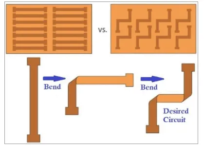
1. Understand the Bend Radius and Bending Areas
The bending area is the heart of a flexible PCB section, and getting it right is crucial to prevent cracking or delamination. The bend radius—the minimum radius a flex area can be bent without damage—depends on the material thickness and the number of layers in the flex section.
As a general rule, the bend radius should be at least 10 times the thickness of the flex material for a single-layer design. For multilayer flex designs, increase this to 15-20 times the thickness. For example, if your flex material is 0.1 mm thick, aim for a bend radius of at least 1.5-2.0 mm in a multilayer setup to avoid stress fractures.
Best Practices for Bending Areas:
- Avoid placing components or vias in the bending areas to prevent stress concentration.
- Use gradual curves instead of sharp angles when designing the flex path. Sharp bends can create weak points.
- Reinforce bending areas with coverlay or additional polyimide layers to enhance durability.
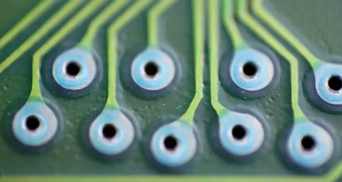
2. Optimize Plated Through-Holes (PTHs) for Reliability
Plated through-holes are essential for connecting different layers in a PCB, but they can be a weak point in rigid-flex designs if not handled properly. PTHs are particularly vulnerable in or near bending areas due to mechanical stress during flexing.
Guidelines for Plated Through-Holes:
- Placement: Keep PTHs out of bending areas. If unavoidable, use teardrop-shaped pads to reduce stress concentration at the via-pad junction.
- Annular Ring Size: Use larger annular rings (at least 0.3 mm wider than the drill diameter) to improve structural integrity. For instance, for a 0.5 mm drill hole, aim for an annular ring of 0.8 mm or more.
- Via Types: Consider using blind or buried vias in flex areas to minimize stress, though this may increase manufacturing costs.
- Plating Thickness: Ensure a copper plating thickness of at least 25 micrometers (1 mil) in PTHs to withstand mechanical stress and maintain electrical conductivity.
By following these guidelines, you can significantly reduce the risk of via cracking or failure in your rigid-flex PCB design.
3. Material Selection for Rigid and Flex Sections
Choosing the right materials is critical for balancing rigidity and flexibility. For the flex sections, polyimide is the most common material due to its excellent thermal stability and flexibility. Rigid sections typically use FR-4 or similar materials for structural support.
Material Guidelines:
- For flex layers, use adhesive-less polyimide to reduce thickness and improve flexibility. A typical thickness for flex layers is 0.05-0.1 mm.
- For rigid sections, FR-4 with a thickness of 0.8-1.6 mm provides sufficient strength for component mounting.
- Ensure proper bonding between rigid and flex layers using no-flow prepreg to prevent delamination during bending.
Material selection also impacts the board’s ability to handle bending stress and thermal expansion, so consult with your manufacturing partner to choose materials suited to your application’s environment.
4. Layer Stack-Up Design for Rigid-Flex PCBs
The layer stack-up defines how rigid and flex sections are arranged in your PCB. A well-planned stack-up ensures signal integrity, minimizes impedance mismatches, and enhances durability.
Stack-Up Tips:
- Keep flex layers in the center of the stack-up to protect them from external stress. For example, in a 6-layer board, place flex layers at positions 3 and 4.
- Avoid abrupt transitions between rigid and flex areas. Use staggered layer transitions to reduce stress points.
- Maintain balanced copper distribution across layers to prevent warping. Aim for a copper fill of 50-70% on each layer.
For high-speed designs, consider controlled impedance in the flex areas. A typical impedance value for high-speed signals is 50 ohms for single-ended traces and 100 ohms for differential pairs. Use trace width and spacing calculators to achieve these values based on your dielectric constant (typically 3.4 for polyimide).
5. Trace Routing in Flex and Transition Areas
Routing traces in a rigid-flex PCB requires special attention, especially in flex and transition areas where mechanical stress is high.
Routing Guidelines:
- Route traces perpendicular to the bend line in flex areas to minimize stress. Avoid diagonal or parallel routing along the bend.
- Use wider traces (at least 0.2 mm) in flex areas to improve durability, even if it means sacrificing some density.
- Add stiffeners or additional coverlay in transition zones between rigid and flex sections to protect traces from stress.
Proper routing ensures that your board can handle repeated bending without trace cracking or signal degradation.
6. Design for Manufacturability (DFM)
A great design is only as good as its manufacturability. Rigid-flex PCBs are complex to produce, so following DFM principles can save time and cost during production.
DFM Tips:
- Keep panel sizes compatible with standard manufacturing processes (typically 18x24 inches or smaller).
- Minimize the number of rigid-flex transitions to simplify fabrication. Each transition adds complexity and cost.
- Specify tolerances clearly. For example, aim for a dimensional tolerance of ±0.1 mm for flex areas to account for bending variations.
Collaborating closely with your manufacturing team during the design phase can help identify potential issues before they become costly problems.
Common Challenges in Rigid-Flex PCB Design
Even with the best guidelines, rigid-flex PCB design can present challenges. Here are some common issues and how to address them:
- Delamination: This occurs when rigid and flex layers separate due to poor bonding or thermal stress. Use compatible materials and proper curing processes to prevent this.
- Signal Integrity Issues: Flex areas can introduce impedance mismatches. Use simulation tools to model signal behavior and adjust trace geometry as needed.
- Mechanical Failure: Repeated bending can lead to cracks in traces or vias. Reinforce critical areas with stiffeners and follow bend radius guidelines.
Applications of Rigid-Flex PCBs
Rigid-flex PCBs are used in a wide range of industries due to their unique combination of durability and flexibility. Some common applications include:
- Consumer Electronics: Smartphones, wearables, and cameras often use rigid-flex designs to save space and improve reliability.
- Medical Devices: Portable diagnostic tools and implantable devices rely on rigid-flex PCBs for their compact size and flexibility.
- Aerospace and Defense: High-reliability applications in harsh environments benefit from the reduced weight and robust performance of rigid-flex boards.
Conclusion: Building Better Rigid-Flex PCBs
Designing a rigid-flex PCB can be a complex task, but by following these guidelines, you can create boards that are both reliable and efficient. Focus on optimizing bending areas with proper bend radius and material choices, ensure plated through-holes are placed and designed for durability, and always consider manufacturability to streamline production.
With careful planning and attention to detail, your rigid-flex PCB design will meet the demands of even the most challenging applications. Start implementing these best practices in your next project to achieve superior performance and longevity in your electronic designs.


