 ALLPCB


Designing high-density printed circuit boards (PCBs) is no easy task for electrical engineers. With the push for smaller, faster, and more powerful electronics, high-density PCB component spacing becomes a critical factor. But what are the biggest hurdles in PCB component placement issues, and how can you tackle them effectively? In this blog, we’ll dive into the top 5 challenges of high-density PCB design and provide practical solutions using component placement optimization techniques, DFM for high-density PCBs, and tips for minimizing signal interference in dense PCBs. Whether you’re working on a compact IoT device or a high-speed server board, these insights will help you achieve a reliable and efficient design.
Let’s explore these challenges in detail, breaking down the technical barriers and offering actionable strategies to overcome them. By the end of this post, you’ll have a clear roadmap to improve your PCB layouts and ensure optimal performance.
Why High-Density PCB Component Placement Matters
High-density PCBs are the backbone of modern electronics, enabling compact designs in smartphones, medical devices, and automotive systems. However, packing more components into a smaller space creates unique challenges. Issues like signal interference, PCB thermal management, and manufacturing constraints can lead to performance failures or costly redesigns if not addressed early. For electrical engineers, mastering high-density PCB component spacing is essential to meet design specs and ensure reliability.
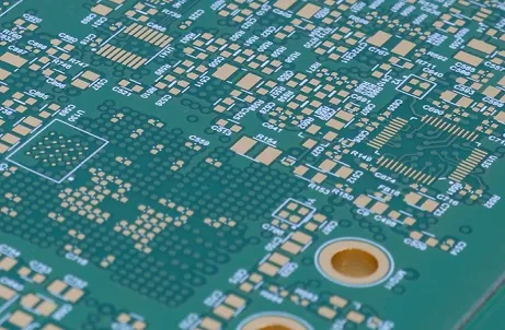
Before we dive into the specific challenges, let’s visualize the complexity of a high-density board.
Challenge 1: Limited Space for Component Placement
One of the most obvious PCB component placement issues in high-density designs is the sheer lack of space. As devices shrink, engineers must fit more components—such as microcontrollers, capacitors, and connectors—into tiny footprints. For example, a modern smartphone PCB might need to accommodate over 1,000 components in an area smaller than 10 square inches. This tight spacing often leads to overlapping parts or insufficient clearance for routing traces.
Solution: Strategic Component Grouping and Layer Stacking
To overcome this, use component placement optimization techniques by grouping related components together. Place high-speed components like processors and memory chips close to each other to minimize trace lengths and reduce latency. Additionally, leverage multi-layer PCBs to stack components vertically. A 6-layer or 8-layer PCB board can provide extra routing space, allowing you to distribute components across layers while maintaining a compact footprint.
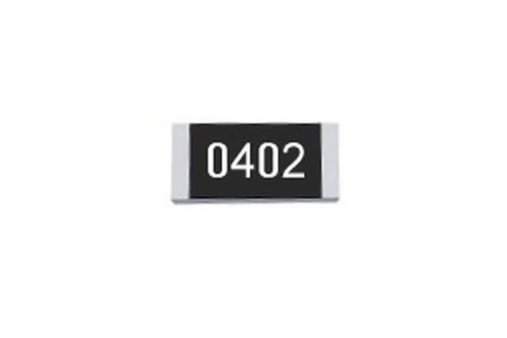
Another tip is to prioritize smaller surface-mount devices (SMDs) over through-hole components. SMDs, such as 0402 or 0201 resistors, take up less space and are ideal for dense designs. Use PCB design software with auto-placement features to experiment with layouts and find the most efficient arrangement.
Challenge 2: Signal Integrity and Interference
In high-density PCBs, components are packed so closely that electromagnetic interference (EMI) and crosstalk become significant issues. High-speed signals, such as those operating at 5 GHz or higher in modern communication devices, are especially prone to interference. Without proper planning, minimizing signal interference in dense PCBs becomes a daunting task, leading to data errors or system failures.
Solution: Implement Ground Planes and Controlled Impedance
To address this, incorporate solid ground planes in your PCB stack-up. A dedicated ground layer reduces EMI by providing a low-impedance return path for signals. For instance, in a 4-layer PCB board, dedicate the second layer to ground to shield high-speed traces on adjacent layers. Additionally, use controlled impedance routing for critical signals. Maintain consistent trace widths (e.g., 6 mils for 50-ohm impedance) and avoid sharp bends to prevent signal reflections.
Another effective strategy is to separate analog and digital components. Place sensitive analog circuits away from noisy digital ones to avoid interference. If space constraints make this difficult, use shielding cans or ferrite beads to isolate noisy sections.
Challenge 3: Thermal Management in Dense Layouts
Heat dissipation is a critical concern in high-density PCBs. Components like power regulators or high-performance CPUs can generate significant heat—sometimes exceeding 100°C in extreme cases. When components are placed too closely, heat builds up, risking damage to nearby parts or degrading performance over time.
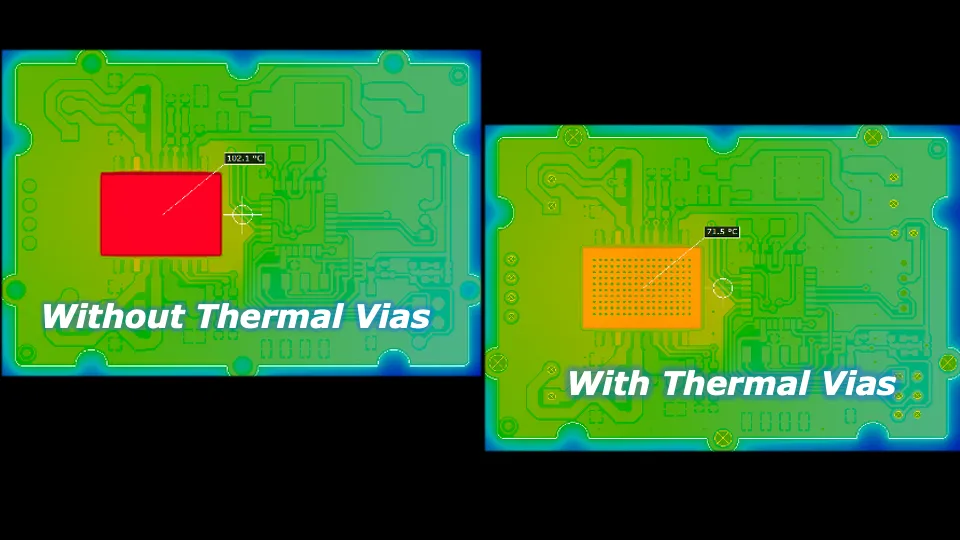
Solution: Optimize Spacing and Add Thermal Relief
While high-density PCB component spacing is limited, strategic placement can help manage heat. Place high-power components near the board edges or areas with better airflow. Use thermal vias—small holes filled with conductive material—to transfer heat from hot components to a copper layer or heat sink. For example, placing 10-15 thermal vias under a power IC can reduce its operating temperature by up to 20°C.
Additionally, consider the thermal conductivity of your PCB material. FR-4, a common substrate, has a thermal conductivity of about 0.3 W/m·K, which may not suffice for high-heat designs. Opt for materials like metal-core PCBs (MCPCBs) with higher conductivity (1-2 W/m·K) for better heat dissipation.
Challenge 4: Manufacturing Constraints and DFM Issues
High-density designs often push the limits of manufacturing capabilities. Tiny component sizes, narrow trace widths (e.g., 3 mils), and tight clearances can lead to fabrication errors or assembly failures. Ignoring DFM for high-density PCBs (Design for Manufacturability) can result in boards that are impossible to produce or prone to defects like solder bridges.
Solution: Follow DFM Guidelines and Collaborate with Manufacturers
Start by adhering to DFM guidelines specific to high-density designs. Ensure minimum spacing between components meets your manufacturer’s capabilities—typically 6-8 mils for standard processes. Use larger pads for fine-pitch components like QFN packages to improve solderability. For example, a 0.5 mm pitch QFN might require pads extended by 0.1 mm beyond the pin for better alignment during assembly.
Collaboration is key. Early in the design phase, consult with your PCB manufacturer to understand their constraints. Many offer DFM checks to identify potential issues before production. Tools like Altium Designer or KiCad also have built-in DFM rules to flag violations during layout.
Challenge 5: Routing Complexity in Dense Designs
Routing traces in a high-density PCB is like solving a complex puzzle. With hundreds of components and limited space, engineers often struggle to route traces without violating design rules or creating long, inefficient paths. This complexity can delay projects and increase the risk of signal integrity issues.
Solution: Use Advanced Routing Tools and HDI Techniques
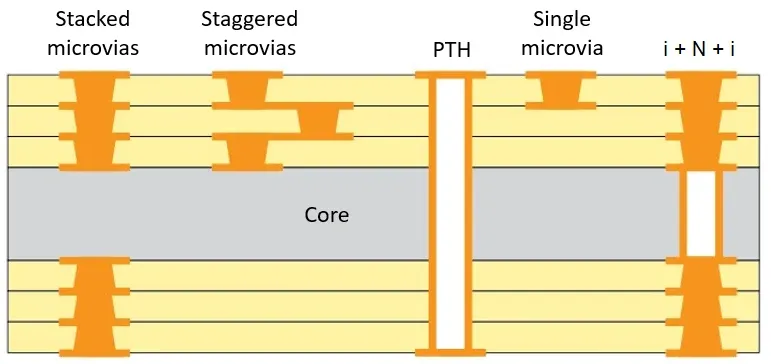
Leverage PCB design software with advanced routing capabilities. Auto-routers can handle initial trace placement, which you can then fine-tune manually for critical nets. High-Density Interconnect (HDI) techniques, such as microvias and blind vias, allow for denser routing by connecting layers without occupying surface space. For instance, microvias with a diameter of 0.1 mm can free up space compared to traditional 0.3 mm drilled vias.
Prioritize critical nets first. Route power and ground traces before signal lines to ensure stable voltage distribution. Keep high-speed traces short and direct, ideally under 1 inch for signals above 1 GHz, to minimize delays and interference.
Best Practices for High-Density PCB Component Placement
Beyond addressing specific challenges, adopting general best practices can elevate your high-density PCB designs:
- Plan Early: Create a rough placement plan before detailed design. Identify critical components and their constraints upfront.
- Use Simulation Tools: Software like SPICE or HyperLynx can simulate signal integrity and thermal performance to catch issues before fabrication.
- Test Iteratively: Build prototypes to validate your design. A small test run can reveal placement flaws that simulations might miss.
- Stay Updated: Manufacturing technologies evolve. Keep learning about new materials and techniques to stay ahead of design challenges.
Conclusion: Mastering High-Density PCB Design
High-density PCB component placement is a balancing act between space constraints, signal integrity, thermal management, manufacturability, and routing complexity. By understanding the top 5 challenges—limited space, signal interference, heat dissipation, DFM issues, and routing difficulties—you can apply targeted solutions to improve your designs. Techniques like multi-layer stacking, ground planes, thermal vias, DFM collaboration, and HDI routing are powerful tools in an engineer’s arsenal for component placement optimization techniques.
As electronics continue to shrink and performance demands grow, mastering high-density PCB component spacing and minimizing signal interference in dense PCBs will remain critical skills. Start implementing these strategies in your next project, and don’t hesitate to reach out to manufacturers or peers for insights.


