 ALLPCB


In the fast-evolving world of electronics, printed circuit boards (PCBs) form the backbone of countless devices, from consumer gadgets to mission-critical aerospace systems. While surface-mount technology (SMT) dominates modern PCB assembly, through-hole assembly remains a vital technique, offering unmatched reliability for specific applications. Despite its origins in the early days of electronics, through-hole assembly continues to play a crucial role in modern PCB manufacturing, blending traditional methods with cutting-edge innovations. This blog explores the enduring relevance of through-hole assembly, its processes, benefits, and applications, providing engineers with practical insights into leveraging this technique for today's designs.
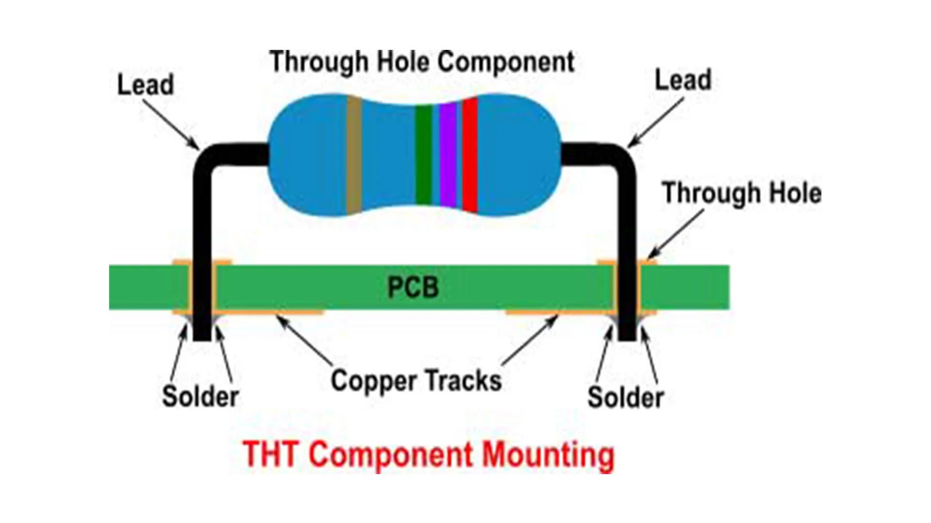
Through-hole assembly involves inserting component leads through drilled holes in a PCB and soldering them to pads on the opposite side. Known for its robust mechanical and electrical connections, this method excels in environments requiring durability, such as automotive, industrial, and military systems. Let's dive into the details of through-hole assembly, its processes, and why it remains a trusted choice for engineers.
What is Through-Hole Assembly?
Through-hole assembly is a PCB manufacturing process where electronic components with wire leads are inserted into pre-drilled holes on the board. These leads are then soldered to conductive pads or traces, creating strong electrical and mechanical connections. Unlike SMT, which places components directly on the board's surface, through-hole components penetrate the board, ensuring greater stability under stress.
The process dates back to the 1950s when PCBs first became widespread. Early through-hole components, like resistors and capacitors, had long leads that were manually inserted and soldered. Today, through-hole assembly supports a wide range of components, including connectors, transformers, and high-power semiconductors, often used in applications where reliability outweighs size constraints.
The Through-Hole Assembly Process
The through-hole assembly process is methodical, combining manual and automated techniques to ensure precision and reliability. Below, we outline the key steps involved:
1. PCB Design and Drilling
The process begins with designing the PCB layout, specifying the placement of through-holes based on component requirements. Holes are drilled using high-precision CNC machines, with diameters typically ranging from 0.1 mm to 6.6 mm, depending on the component lead size. For example, a standard resistor lead might require a 0.8 mm hole, while a larger connector could need a 2 mm hole. Drilling accuracy is critical to ensure proper alignment and avoid signal integrity issues.
2. Component Insertion
Components are inserted into the drilled holes, either manually or using automated insertion machines. Manual insertion is common for low-volume or prototype boards, while automated systems, such as selective soldering machines, are used for high-volume production. Components must be oriented correctly, as misaligned leads can cause electrical faults or mechanical stress.
3. Soldering
Soldering secures the component leads to the PCB. Two primary methods are used:
- Wave Soldering: The PCB passes over a wave of molten solder, which bonds the leads to the pads. This is efficient for high-volume production but requires careful control to prevent solder bridges.
- Hand Soldering: Used for prototypes or low-volume runs, hand soldering offers precision but is time-intensive. Skilled technicians ensure consistent solder joints, typically achieving joint strengths of 5–10 MPa, depending on the solder alloy.
4. Inspection and Testing
After soldering, the PCB undergoes rigorous inspection. Automated optical inspection AOI systems check for solder joint defects, such as voids or incomplete bonds, with defect detection rates often exceeding 95%. Functional testing verifies electrical connectivity, ensuring the board meets design specifications. For high-reliability applications, X-ray inspection may be used to examine hidden solder joints.
Advantages of Through-Hole Assembly
Through-hole assembly offers several advantages that make it indispensable for certain applications. Here are the key benefits:
1. Superior Mechanical Strength
The physical connection of component leads passing through the PCB provides exceptional mechanical stability. For example, a through-hole connector can withstand shear forces up to 100 N, compared to 20–30 N for SMT equivalents. This makes through-hole ideal for components subject to vibration, shock, or thermal cycling, such as in automotive or aerospace systems.
2. High Reliability in Harsh Environments
Through-hole joints are less prone to failure in extreme conditions. In military applications, where PCBs may operate at temperatures from -55°C to 125°C, through-hole components maintain reliable connections, with failure rates as low as 0.01% over 10 years, according to MIL-STD-810 standards.
3. Ease of Repair and Replacement
Through-hole components are easier to desolder and replace than SMT components, reducing repair time and costs. This is critical in industries like medical equipment, where downtime can have serious consequences. For instance, replacing a through-hole capacitor typically takes 2–3 minutes, compared to 5–10 minutes for an SMT equivalent.
4. Support for High-Power Components
High-power components, such as transformers or large electrolytic capacitors, often require through-hole assembly due to their size and heat dissipation needs. These components can handle currents exceeding 10 A or voltages above 500 V, making them unsuitable for SMT.
Challenges of Through-Hole Assembly
Despite its advantages, through-hole assembly has limitations that engineers must consider:
1. Larger Board Size
Through-hole components require more space due to drilled holes and larger component footprints. This can increase board size by 20–30% compared to SMT designs, making it less suitable for compact devices like smartphones.
2. Higher Assembly Costs
The process is labor-intensive, especially for hand soldering, leading to higher costs. For example, assembling a through-hole PCB with 100 components might cost $50–$100 more than an SMT equivalent due to additional labor and material requirements.
3. Limited Automation
While wave soldering automates high-volume production, low-volume or complex boards often rely on manual insertion and soldering, reducing scalability. Automation rates for through-hole assembly typically reach 70–80%, compared to 95% for SMT.
Applications of Through-Hole Assembly in Modern PCBs
Through-hole assembly remains a cornerstone in industries where reliability and durability are paramount. Here are some key applications:
1. Automotive Electronics
In automotive systems, PCBs must withstand vibrations, temperature fluctuations, and high currents. Through-hole assembly is used for power modules, sensors, and connectors, ensuring reliable performance in engine control units (ECUs) that operate at 12–48 V and currents up to 50 A.
Suggested Reading: A Beginner's Guide to Through-Hole Assembly for Electronics Projects
2. Aerospace and Defense
Aerospace PCBs require faultless operation in extreme conditions. Through-hole components, such as ruggedized connectors and high-power resistors, are used in avionics and satellite systems, where signal integrity at frequencies up to 10 GHz is critical.
3. Industrial Equipment
Heavy-duty industrial equipment, like motor drives and power supplies, relies on through-hole assembly for components handling high voltages (e.g., 600 V) and currents (e.g., 20 A). These systems demand robust connections to prevent failures in harsh environments.
4. Prototyping and Education
Through-hole assembly is widely used in PCB prototyping and educational settings due to its ease of soldering and component replacement. Hobbyists and students often work with through-hole kits, such as Arduino boards, which use 2.54 mm pitch headers for accessibility.
Modern Innovations in Through-Hole Assembly
While through-hole assembly is a traditional technique, recent advancements have enhanced its efficiency and applicability:
1. Selective Soldering
Selective soldering machines target specific through-hole components, reducing thermal stress on the board. These systems achieve soldering precision within 0.1 mm, improving quality for mixed-technology PCBs that combine through-hole and SMT components.
2. Lead-Free Soldering
Environmental regulations, such as RoHS, have driven the adoption of lead-free solders, like SAC305 (96.5% tin, 3% silver, 0.5% copper). These alloys maintain joint strength (approximately 7 MPa) while reducing environmental impact, aligning with sustainable manufacturing trends.
3. Compact Through-Hole Packages
Component manufacturers have developed smaller through-hole packages, such as low-profile connectors with 1.5 mm pitch, allowing denser designs without sacrificing reliability. These advancements enable through-hole assembly to compete with SMT in space-constrained applications.
4. Automated Inspection
Advanced AOI and X-ray systems have improved defect detection, with modern machines identifying solder joint issues at resolutions as fine as 10 µm. This ensures high reliability, even in complex through-hole assemblies.
Integrating Through-Hole and SMT: Hybrid PCBs
Many modern PCBs combine through-hole and SMT to leverage the strengths of both technologies. Hybrid PCBs use SMT for compact, high-density components and through-hole for high-power or mechanically stressed components. For example, a telecommunications board might use SMT for microchips and through-hole for RF connectors handling signals at 5 GHz.
Designing hybrid PCBs requires careful planning to balance manufacturing processes. Engineers must ensure thermal profiles during soldering are compatible, as through-hole components typically require higher temperatures (e.g., 260°C for lead-free solder) than SMT components (e.g., 250°C). Advanced PCB design software, like Altium Designer, helps optimize layouts for hybrid assemblies, minimizing signal interference and ensuring manufacturability.
How ALLPCB Supports Through-Hole Assembly
For engineers seeking reliable through-hole assembly, ALLPCB offers comprehensive solutions tailored to modern PCB needs. Our advanced manufacturing facilities support both high-volume production and quick-turn prototyping, delivering through-hole PCBs with precision and efficiency. With global logistics and a robust supply chain, we ensure timely delivery of components and boards, even for complex designs requiring hybrid SMT and through-hole assemblies. Our state-of-the-art inspection systems, including AOI and X-ray, guarantee defect-free solder joints, meeting stringent industry standards like IPC-A-610. Whether you're developing automotive ECUs or aerospace systems, ALLPCB's expertise helps bring your designs to life with unmatched quality.
Conclusion: The Enduring Value of Through-Hole Assembly
Through-hole assembly remains a cornerstone of PCB manufacturing, offering unmatched reliability for applications where durability and performance are non-negotiable. While SMT dominates compact, high-volume production, through-hole's robust connections and ease of repair make it indispensable in automotive, aerospace, and industrial sectors. Modern innovations, like selective soldering and lead-free alloys, have further enhanced its efficiency, ensuring its relevance in today's fast-paced electronics industry.
By understanding the strengths and challenges of through-hole assembly, engineers can make informed decisions about when to use this technique, whether standalone or in hybrid designs. With its proven track record and ongoing advancements, through-hole assembly continues to bridge traditional craftsmanship with the demands of modern PCBs, powering the devices that shape our world.


