 ALLPCB


If you're looking to understand the ins and outs of PCB assembly, you've come to the right place. This guide will walk you through the complete PCB assembly process flow, explore cutting-edge PCB assembly technologies like SMT, share essential PCB assembly best practices, and provide a detailed PCB assembly design guide. Whether you're an engineer, designer, or manufacturer, this comprehensive resource will help you achieve high-quality results with actionable insights.
At ALLPCB, we’re committed to supporting your projects with top-tier solutions. Let’s dive into the world of PCB assembly and uncover the steps, tools, and tips that can elevate your electronic designs.
What Is PCB Assembly? A Quick Overview
PCB assembly, often abbreviated as PCBA, is the process of attaching electronic components to a printed circuit board (PCB) to create a functional electronic device. It transforms a bare PCB into a fully operational unit by soldering components onto designated pads or through holes. This process is critical in industries ranging from consumer electronics to aerospace, where reliability and precision are non-negotiable.
In this guide, we’ll break down every aspect of PCB assembly, ensuring you have the knowledge to optimize your designs and production workflows. From the step-by-step assembly process to advanced technologies and design tips, we’ve got you covered.
Understanding the PCB Assembly Process Flow
The PCB assembly process flow is a structured sequence of steps that ensures components are accurately placed and secured on the board. Following a well-defined workflow minimizes errors and ensures the final product meets quality standards. Here’s a detailed look at each stage:
1. Design and Preparation
Before assembly begins, the PCB design must be finalized. This includes creating a schematic and layout using design software, ensuring proper placement of components, and generating manufacturing files like Gerber files and a Bill of Materials (BOM). Thorough preparation at this stage prevents costly mistakes during assembly.
2. Stencil Printing (Solder Paste Application)
For surface mount technology (SMT), the process starts with applying solder paste to the PCB using a stencil. The stencil ensures that paste is deposited only on the pads where components will be placed. Precision here is key, as uneven paste can lead to poor solder joints.
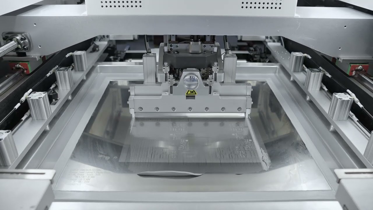
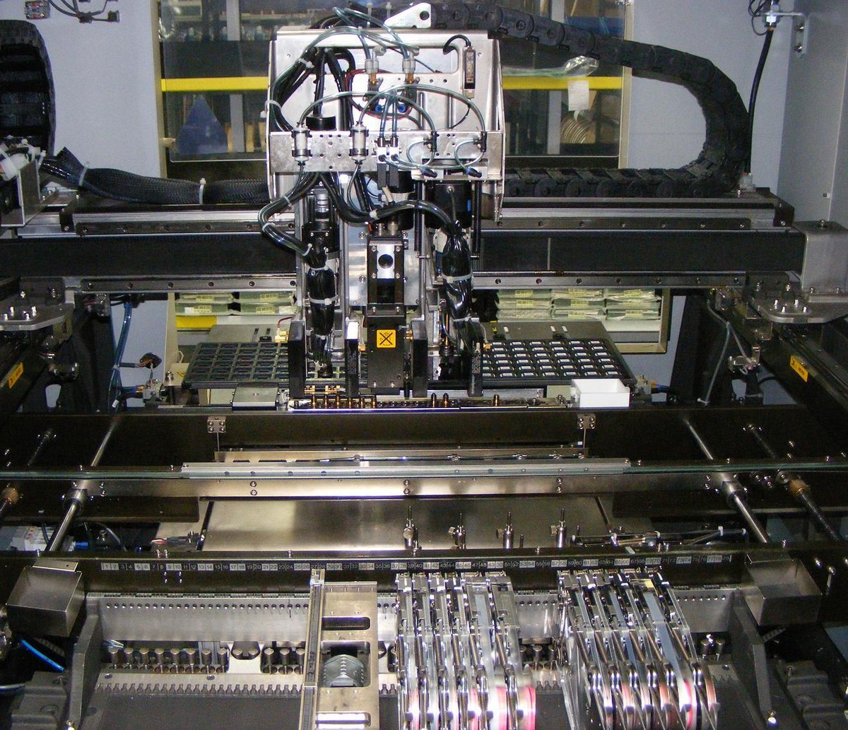
3. Component Placement
Next, components are placed onto the PCB. For SMT, automated pick-and-place machines are used to position tiny components with high accuracy, often at speeds of thousands of placements per hour. For through-hole components, manual or semi-automated placement may be used.
4. Reflow Soldering (For SMT)
Once components are placed, the PCB passes through a reflow oven. The oven heats the board to melt the solder paste, creating strong electrical and mechanical connections between components and pads. Temperature profiles are carefully controlled to avoid thermal damage—for instance, peak temperatures often reach around 240-260°C for lead-free solder.
5. Wave Soldering (For Through-Hole)
For through-hole components, wave soldering is often used. The PCB passes over a wave of molten solder, which adheres to the exposed metal areas. This method is efficient for boards with a mix of SMT and through-hole parts.
6. Inspection and Testing
After soldering, the assembled PCB undergoes inspection. Automated Optical Inspection (AOI) systems check for misaligned components or defective solder joints. Functional testing ensures the board operates as intended, often involving power-up tests and signal integrity checks at specific frequencies (e.g., testing for signal speeds up to 5 GHz for high-speed designs).
7. Final Assembly and Packaging
Once tested, the PCB may be integrated into a larger system or encased in a protective housing. It’s then packaged for shipping, with anti-static materials to prevent electrostatic discharge (ESD) damage.
Understanding this PCB assembly process flow helps in planning and optimizing production timelines. Each step requires precision to ensure the final product is reliable and functional.
Exploring PCB Assembly Technologies: SMT and Beyond
The world of PCB assembly technologies has evolved rapidly, with SMT (Surface Mount Technology) leading the way in modern electronics manufacturing. Let’s explore the key technologies shaping the industry and their benefits.
Surface Mount Technology (SMT)
SMT is the most widely used PCB assembly technology today. Unlike through-hole technology, SMT components are mounted directly onto the surface of the PCB, allowing for smaller, denser, and more efficient designs. Here are some advantages of SMT:
- Compact Designs: SMT components are much smaller, enabling high-density layouts critical for devices like smartphones and wearables.
- High-Speed Production: Automated SMT assembly lines can place components at rates of up to 100,000 per hour, significantly reducing production time.
- Cost-Effectiveness: Reduced material usage and faster assembly lower overall costs, especially for large-scale production.
However, SMT requires precise design and manufacturing processes. For instance, pad sizes must match component footprints exactly—often within tolerances of 0.1 mm—to avoid soldering defects.
Through-Hole Technology (THT)
While SMT dominates, Through-Hole Technology (THT) remains relevant for applications requiring durability, such as power electronics or industrial equipment. THT components have leads that pass through holes in the PCB and are soldered on the opposite side, providing stronger mechanical bonds. However, THT is slower and less suited for compact designs.
Mixed Assembly
Many modern PCBs use a combination of SMT and THT to balance performance and durability. For example, a board might use SMT for microcontrollers and capacitors, while using THT for connectors that experience mechanical stress.
Advanced Technologies: Microvias and HDI
For high-density interconnect (HDI) boards, technologies like microvias (vias with diameters less than 0.15 mm) are used to connect multiple layers in a compact space. These advancements are critical for high-speed applications, where signal integrity at frequencies above 1 GHz is a priority.
By leveraging these PCB assembly technologies like SMT, manufacturers can meet the demands of modern electronics, balancing speed, cost, and performance.
PCB Assembly Best Practices for Optimal Results
Adhering to PCB assembly best practices ensures high-quality outcomes and minimizes production issues. Here are proven strategies to follow during design and assembly:
1. Prioritize Design for Manufacturability (DFM)
Design your PCB with manufacturing in mind. This means ensuring component spacing adheres to assembly tolerances (e.g., a minimum of 0.2 mm between SMT components) and avoiding overly complex layouts that could lead to errors during production.
2. Use Standard Components
Opt for widely available components with standard footprints. Custom or obsolete parts can delay production and increase costs. Check availability and lead times during the design phase.
3. Implement Proper Thermal Management
Heat dissipation is critical, especially for high-power designs. Use thermal vias (with diameters of 0.3-0.5 mm) under components like power ICs to transfer heat to ground planes, preventing overheating during operation.
4. Minimize Signal Interference
For high-speed designs, maintain controlled impedance on traces (e.g., 50 ohms for RF signals) and keep signal paths short to reduce crosstalk. Place decoupling capacitors close to IC power pins to filter noise.
5. Conduct Thorough Testing
Don’t skip post-assembly testing. Use AOI to catch visual defects and in-circuit testing (ICT) to verify electrical performance. For critical applications, perform environmental testing to ensure reliability under varying conditions, such as temperatures from -40°C to 85°C.
Following these PCB assembly best practices can significantly reduce defects, improve yield rates, and ensure your boards perform reliably in the field.
PCB Assembly Design Guide: Tips for Success
Designing a PCB for assembly is just as important as the assembly process itself. A well-thought-out design minimizes errors and ensures smooth production. Here’s a practical PCB assembly design guide to help you create manufacturable and reliable boards.
1. Optimize Component Placement
Place components logically, grouping related parts together to minimize trace lengths. For SMT, ensure components are oriented consistently to simplify automated assembly. Keep at least 2 mm clearance around large components for rework access.
2. Design for Automated Assembly
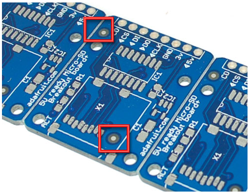
Automated pick-and-place machines require fiducial markers on the PCB for alignment. Include at least three fiducials, ideally 1 mm in diameter, placed diagonally across the board for optimal accuracy.
3. Follow Trace and Via Guidelines
Ensure trace widths are sufficient for the current they carry. For example, a 10-mil (0.254 mm) trace can handle approximately 1 A of current at 1 oz copper thickness. Use vias with appropriate diameters (e.g., 0.3 mm for standard signals) to avoid manufacturing issues.
4. Include Clear Documentation
Provide detailed assembly drawings and a BOM with part numbers, quantities, and reference designators. Clear documentation prevents miscommunication between design and manufacturing teams.
5. Account for Panelization
If producing multiple PCBs, design for panelization to optimize manufacturing efficiency. Include breakaway tabs or V-scoring with a minimum width of 0.3 mm to separate boards post-assembly without damage.
By following this PCB assembly design guide, you can create boards that are easier to assemble, test, and deploy, ultimately saving time and resources.
Common Challenges in PCB Assembly and How to Overcome Them
Even with careful planning, challenges can arise during PCB assembly. Here are some common issues and solutions to address them:
1. Solder Joint Defects
Issues like cold solder joints or bridging can occur due to incorrect reflow profiles or poor paste application. Use a reflow profile with a gradual ramp-up (e.g., 1-3°C per second) to ensure proper melting and adhesion.
2. Component Misalignment
Misaligned components often result from inaccurate pick-and-place setups or missing fiducials. Verify machine calibration and include clear fiducial markers to improve placement accuracy to within 0.05 mm.
3. Thermal Damage
Excessive heat during soldering can damage sensitive components. Adhere to manufacturer-recommended thermal profiles, ensuring peak temperatures don’t exceed component limits (often around 260°C for 10 seconds).
Proactive measures and attention to detail can mitigate these challenges, ensuring a smoother assembly process.
Why Choose ALLPCB for Your PCB Assembly Needs?
At ALLPCB, we understand the complexities of PCB assembly and are dedicated to providing seamless, high-quality solutions. Our state-of-the-art facilities support both SMT and THT assembly, with rigorous quality control at every step. Whether you need prototype runs or full-scale production, our team ensures precision, reliability, and fast turnaround times.
We also offer comprehensive design support to help you optimize your PCB for manufacturing. With advanced technologies and a commitment to excellence, we’re your trusted partner for bringing electronic innovations to life.
Conclusion: Mastering PCB Assembly for Success
PCB assembly is a intricate yet essential process that determines the functionality and reliability of electronic devices. By understanding the PCB assembly process flow, leveraging advanced PCB assembly technologies like SMT, adhering to PCB assembly best practices, and following a detailed PCB assembly design guide, you can achieve outstanding results in your projects.
From design optimization to final testing, every step plays a critical role in ensuring quality. With the insights provided in this guide, you’re well-equipped to tackle the challenges of PCB assembly and create products that meet the highest standards. Partner with ALLPCB to streamline your journey from concept to creation, and experience the difference that expertise and dedication can make.


