 ALLPCB


Are you wondering what lies ahead for PCB depaneling? The future of PCB depaneling is rapidly evolving with cutting-edge technologies like AI, automation, and advanced depaneling methods. These innovations promise higher precision, faster production, and reduced costs for electrical engineers and manufacturers. In this blog, we’ll dive deep into the emerging trends and technologies shaping the next generation of depaneling, including AI-driven solutions and automated visual inspection systems. Let’s explore how these advancements can impact your work and keep you ahead in the electronics industry.
Introduction to PCB Depaneling and Its Importance
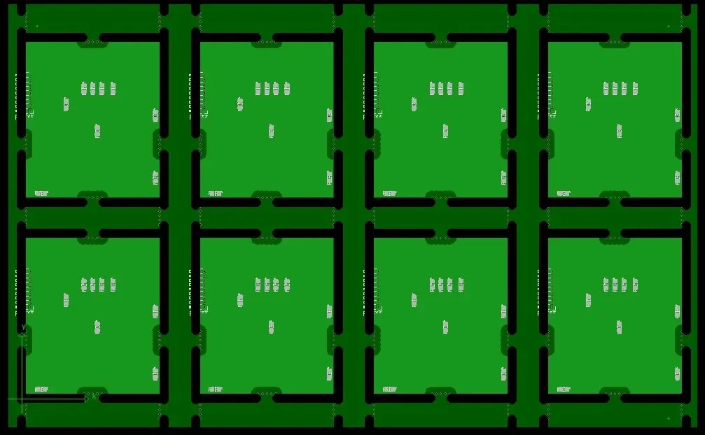
Printed Circuit Board (PCB) depaneling is a critical step in electronics manufacturing. It involves separating individual PCBs from a larger panel after assembly. This process ensures that each board is ready for final integration into devices like smartphones, automotive systems, or medical equipment. For electrical engineers, achieving clean cuts without damaging delicate components or traces is essential. Traditional methods like manual breaking or mechanical routing often risk stress on the board, leading to cracks or failures.
As demand for smaller, more complex electronics grows, so does the need for precise and efficient depaneling. The future of PCB depaneling lies in technologies that minimize human error, boost throughput, and handle intricate designs. In this post, we’ll break down the trends and tools—such as advanced depaneling methods and AI depaneling—that are set to redefine this process for engineers like you.
Why the Future of PCB Depaneling Matters to Electrical Engineers
As an electrical engineer, you’re likely dealing with tighter design constraints and faster production cycles. The push for miniaturization means PCBs are packed with components, leaving little room for error during depaneling. A single damaged trace can lead to signal integrity issues, with impedance mismatches potentially disrupting performance at high frequencies (e.g., above 1 GHz). Moreover, industries like automotive and aerospace demand reliability—think of a PCB in an electric vehicle control unit failing due to a depaneling flaw.
Emerging technologies in depaneling address these challenges head-on. They offer solutions that not only improve precision but also integrate seamlessly into automated production lines. Staying updated on the future of PCB depaneling can help you select the right tools, reduce scrap rates, and meet strict quality standards. Let’s look at the key trends driving this transformation.
Key Trends Shaping the Future of PCB Depaneling
1. Rise of Advanced Depaneling Methods
Traditional depaneling methods like V-scoring and mechanical routing are giving way to advanced depaneling methods that prioritize precision and flexibility. Laser depaneling, for instance, uses focused beams to cut PCBs with minimal mechanical stress. This method is ideal for thin, flexible PCBs or those with high component density, as it avoids vibration-induced damage. Studies suggest laser depaneling can achieve cut tolerances as tight as ±25 micrometers, compared to ±100 micrometers for mechanical methods.
Another promising approach is water jet cutting, which uses high-pressure water streams mixed with abrasives to slice through materials. While less common, it’s gaining traction for its ability to handle thicker boards without thermal damage—a key concern with laser systems. For engineers, these advanced depaneling methods mean less rework and higher yield, especially in high-stakes applications.

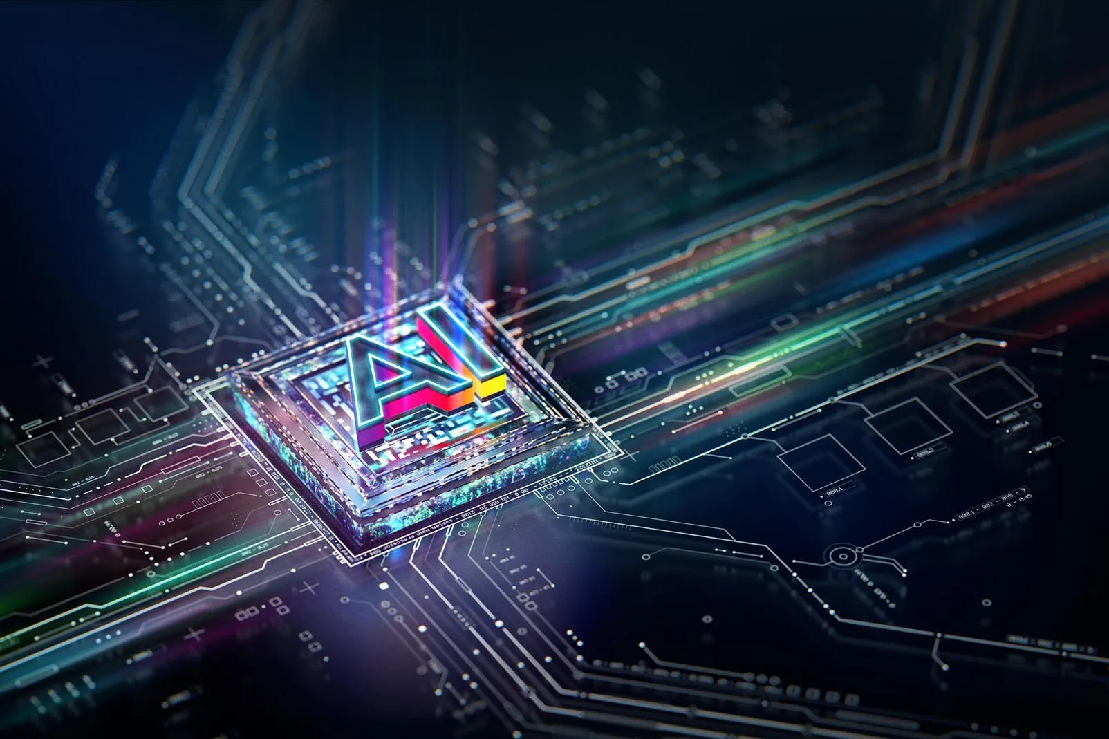
2. AI Depaneling: Smarter Systems for Better Results
Artificial Intelligence (AI) is making waves in PCB manufacturing, and depaneling is no exception. AI depaneling systems use machine learning algorithms to optimize cutting paths, detect board variations, and predict potential defects before they occur. Imagine a system that analyzes a PCB panel’s layout in real-time, adjusting the cutting process to avoid overstressing a densely populated area. This isn’t science fiction—it’s happening now.
For example, AI can reduce material waste by calculating the most efficient depaneling sequence, potentially cutting scrap rates by up to 15%. It can also integrate with sensors to monitor cutting tool wear, ensuring consistent performance over long production runs. For electrical engineers, AI depaneling means less manual oversight and more reliable outcomes, even with complex designs. As reported in recent industry updates, companies like Laser Photonics are actively expanding R&D in AI-driven depaneling systems to enhance precision and throughput.
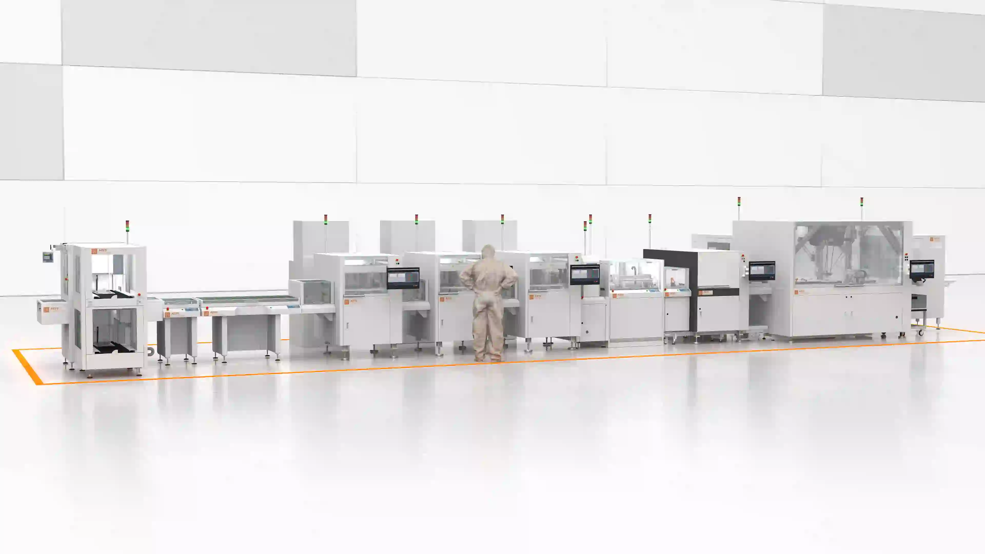
3. Next Generation Depaneling with Automation
Next generation depaneling is all about automation. Fully automated depaneling machines are becoming the norm, especially in high-volume production environments. These systems can handle everything from loading panels to separating individual boards and sorting them for the next assembly stage. With speeds reaching up to 100 boards per minute in some setups, automation slashes production time while maintaining consistency.
Automation also integrates with Industry 4.0 principles, allowing machines to communicate with other equipment on the factory floor. For instance, a depaneling system might receive real-time data from an upstream assembly line to adjust its operation based on incoming panel specifications. For engineers, this level of connectivity means fewer bottlenecks and easier scalability—crucial when ramping up production for a new product launch.
According to market insights, the global PCB depaneling systems market is projected to grow at a CAGR of 6.6% from 2025 to 2033, driven largely by automation in industries like consumer electronics and automotive.
Suggested Reading: Automated Depaneling vs. Manual Breakaway: Which Method is Right for You?
4. Automated Visual Inspection for Quality Assurance
Quality control is a cornerstone of PCB manufacturing, and automated visual inspection (AVI) is revolutionizing how engineers ensure depaneling accuracy. AVI systems use high-resolution cameras and image processing software to inspect cuts, edges, and component placement after depaneling. These systems can detect defects as small as 10 micrometers, far beyond human capability, ensuring that no damaged board slips through.
For electrical engineers, AVI offers a way to maintain high standards without slowing down production. Modern systems can process up to 200 images per second, flagging issues like jagged edges or misaligned cuts in real-time. Some even incorporate AI to learn from past inspections, improving detection accuracy over time. This technology is especially valuable when working on high-frequency boards where a minor edge defect could disrupt signal integrity at speeds above 5 Gbps.
Posts on social platforms like X highlight growing interest in AVI, with manufacturers showcasing how deep-learning algorithms enhance defect detection in PCB assembly. This trend is set to grow as more companies adopt smart manufacturing solutions.
5. Sustainability and Material Innovations
The future of PCB depaneling isn’t just about speed and precision—it’s also about sustainability. Manufacturers are under pressure to reduce waste and energy consumption. Advanced depaneling methods like laser cutting already minimize material loss, but new biodegradable substrates and recyclable materials are emerging as game-changers. These materials require depaneling systems that can adapt to different mechanical properties without compromising cut quality.
Additionally, energy-efficient machines are being developed to lower the carbon footprint of production. For engineers, this means balancing performance with environmental responsibility, especially if your company targets eco-conscious markets. Staying informed about material trends can help you design PCBs that are both cutting-edge and sustainable.
Challenges in Adopting New Depaneling Technologies
While the future of PCB depaneling is exciting, it’s not without hurdles. High initial costs for advanced systems like laser or AI depaneling setups can be a barrier, especially for small to medium-sized enterprises. A single laser depaneling machine can cost upwards of $100,000, compared to $10,000 for a basic mechanical router. Engineers may need to justify this investment by demonstrating long-term savings in reduced scrap and labor costs.
Another challenge is the learning curve. Operating next generation depaneling equipment often requires specialized training, and integrating these systems into existing workflows can disrupt production temporarily. For instance, syncing an automated depaneling line with older assembly machines might require custom software or hardware tweaks. Planning for these transitions is key to avoiding costly downtime.
Lastly, compatibility with diverse PCB designs remains an issue. Not all advanced depaneling methods suit every board type—laser cutting, for example, may cause thermal damage to certain materials if not calibrated properly. As an engineer, you’ll need to evaluate which technology aligns best with your specific projects.
How Electrical Engineers Can Prepare for the Future
So, how can you stay ahead in this fast-changing field? Here are actionable steps to prepare for the future of PCB depaneling:
- Invest in Training: Upskill yourself and your team on advanced depaneling methods and automation software. Many equipment suppliers offer workshops or online courses.
- Collaborate with Manufacturers: Work closely with depaneling equipment providers to customize solutions for your production needs. This can help you address unique challenges like handling ultra-thin boards.
- Test New Technologies: Start small by piloting AI depaneling or automated visual inspection systems on a single production line. Use data from these trials to build a case for wider adoption.
- Stay Updated: Follow industry reports and join forums to keep track of emerging trends. Resources like market research on PCB depaneling systems can provide valuable insights into growth areas.
Conclusion: Embracing the Future of PCB Depaneling
The future of PCB depaneling is bright, with advanced depaneling methods, AI depaneling, and automated visual inspection leading the charge. These technologies offer electrical engineers the tools to achieve unparalleled precision, efficiency, and quality in PCB production. Whether you’re working on consumer electronics, automotive systems, or aerospace applications, staying ahead of these trends can give you a competitive edge.
While challenges like cost and compatibility exist, the long-term benefits of adopting next generation depaneling solutions are clear. Reduced waste, faster throughput, and improved reliability are just a few of the rewards awaiting those who embrace innovation. So, take the first step—explore these technologies, test them in your workflows, and prepare for a future where PCB depaneling is smarter, faster, and more sustainable than ever before.


