 ALLPCB


If you're looking to understand the ins and outs of rigid-flex board assembly, you're in the right place. This guide covers everything from the basics of rigid-flex PCB design to the detailed assembly process, challenges, material selection, and testing methods. Whether you're an engineer or a designer, you'll find actionable insights to help you navigate the complexities of rigid-flex technology and create reliable, high-performance boards for your projects.
At ALLPCB, we’re committed to supporting your journey with comprehensive resources and expertise. Let’s dive into this complete guide to rigid-flex board assembly and explore each critical aspect step by step.
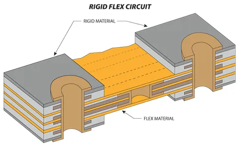
What Are Rigid-Flex PCBs?
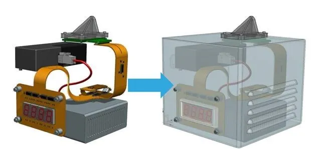
Rigid-flex PCBs combine the stability of rigid circuit boards with the adaptability of flexible circuits. This hybrid design allows for compact, lightweight, and durable electronic solutions that can bend and fold without breaking. These boards are widely used in industries like aerospace, medical devices, automotive, and consumer electronics, where space constraints and reliability are critical.
A typical rigid-flex PCB consists of multiple layers of rigid and flexible substrates bonded together. The rigid sections provide structural support for components, while the flexible sections enable dynamic movement or fit into tight spaces. This unique combination reduces the need for connectors and cables, improving signal integrity and reducing assembly costs.
Key Benefits of Rigid-Flex PCBs
Before we dive into the assembly process, let’s look at why rigid-flex PCBs are a popular choice:
- Space Efficiency: The ability to fold and bend allows rigid-flex boards to fit into compact designs, saving up to 60% of space compared to traditional rigid boards.
- Enhanced Reliability: Fewer connectors and solder joints mean a lower risk of failure, making these boards ideal for high-vibration environments.
- Cost-Effectiveness: While initial design costs may be higher, the reduction in connectors and assembly steps can lower overall production costs by 20-30% in some cases.
- Improved Signal Integrity: Direct connections between rigid and flex sections reduce signal loss, supporting high-speed applications with impedance control as tight as ±10%.
Rigid-Flex PCB Design: Laying the Foundation
The success of rigid-flex board assembly starts with a well-thought-out design. Rigid-flex PCB design requires careful planning to ensure functionality, manufacturability, and durability. Here are the key considerations:
1. Define Bend Areas and Radius
Identify where the board will bend and calculate the minimum bend radius to avoid stress on the flexible layers. A general rule is to maintain a bend radius of at least 10 times the thickness of the flex layer (e.g., a 0.1 mm thick flex layer requires a 1 mm bend radius) to prevent cracking.
2. Layer Stack-Up Planning
Design the stack-up to balance rigid and flexible sections. Use thinner materials in flex areas (like 1-2 mil polyimide) and ensure transitions between rigid and flex zones are gradual to avoid delamination. Typically, a 4- to 6-layer stack-up is common for rigid-flex designs in consumer electronics.
3. Component Placement
Place components only on rigid sections to avoid stress on solder joints during bending. Keep a clearance of at least 0.5 mm between components and flex areas to prevent mechanical interference.
Rigid-Flex PCB Assembly Process: Step by Step
The rigid-flex PCB assembly process is more complex than traditional PCB assembly due to the combination of materials and the need for precision. Below is a detailed breakdown of the steps involved:
1. Material Preparation
The process begins with preparing rigid and flexible materials. Rigid sections often use FR-4 with thicknesses of 0.8-1.6 mm, while flexible sections use polyimide films of 1-3 mils. These materials are cut to size and cleaned to remove contaminants.
2. Lamination
Rigid and flexible layers are bonded using adhesives like no-flow prepreg or acrylic adhesives. The lamination process occurs under controlled heat (around 180°C) and pressure (up to 300 psi) to ensure a strong bond without air bubbles.
3. Drilling and Plating
Holes are drilled for vias and component mounting. Due to the material differences, drilling speeds are adjusted (e.g., 50,000 RPM for rigid areas, slower for flex) to prevent tearing. Copper plating follows to create conductive paths, often achieving a thickness of 1-2 oz per square foot.
4. Circuit Patterning
Photolithography is used to etch copper traces on both rigid and flex sections. Etching factors must account for different copper thicknesses (e.g., 0.5 oz for flex, 1 oz for rigid) to ensure precise lines and spaces, often as tight as 3 mils.
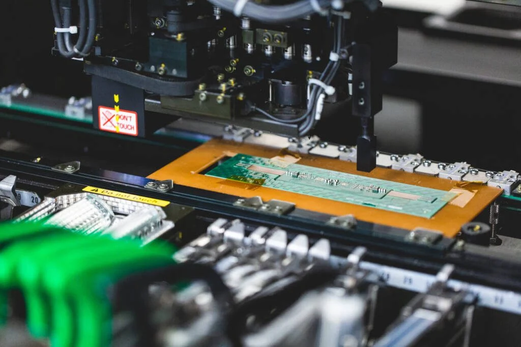
5. Component Assembly
Surface-mount technology (SMT) is commonly used for component placement on rigid sections. Solder paste is applied, components are placed with pick-and-place machines, and reflow soldering (at temperatures of 240-260°C) secures them in place. Flexible areas are typically left unpopulated to maintain flexibility.
6. Final Assembly and Shaping
The board is cut to its final shape using laser or mechanical routing. Stiffeners may be added to flex areas for extra support during handling. The board is then cleaned and prepared for testing.
Challenges of Rigid-Flex PCB Assembly
While rigid-flex boards offer many advantages, the challenges of rigid-flex PCB assembly can’t be overlooked. Addressing these issues early can save time and costs:
1. Material Compatibility
Different thermal expansion rates between rigid (FR-4, CTE of 14-17 ppm/°C) and flexible materials (polyimide, CTE of 20-25 ppm/°C) can cause delamination or cracking during thermal cycles. Careful material selection and adhesive choice are crucial.
2. Complex Manufacturing
The transition zones between rigid and flex areas are prone to stress. Misalignment during lamination or improper drilling can lead to failures, increasing scrap rates by up to 15% in some production runs if not managed properly.
3. Higher Costs
Rigid-flex assembly often costs 2-3 times more than standard rigid PCB assembly due to specialized materials, equipment, and longer production times. Small batch runs can be particularly expensive.
4. Design Constraints
Engineers must balance flexibility with durability. Over-bending or placing components too close to flex areas can cause mechanical failure, with studies showing a 30% failure rate in poorly designed bend zones under repeated stress.
Material Selection for Rigid-Flex PCBs
Material selection for rigid-flex PCBs plays a critical role in performance and reliability. Here’s what to consider when choosing materials:
1. Flexible Substrate
Polyimide is the most common choice for flexible layers due to its high thermal stability (up to 400°C) and flexibility. It’s available in thicknesses from 1 to 5 mils, with thinner options preferred for tighter bend radii.
2. Rigid Substrate
FR-4 is widely used for rigid sections due to its cost-effectiveness and mechanical strength. For high-frequency applications, materials like PTFE or high-Tg FR-4 (Tg > 170°C) are chosen to maintain signal integrity at speeds above 5 GHz.
3. Copper Foil
Rolled annealed (RA) copper is preferred for flexible areas due to its ductility, while electrodeposited (ED) copper works well for rigid sections. Thickness typically ranges from 0.5 to 2 oz, depending on current-carrying needs.
4. Adhesives and Coverlays
No-flow prepreg or acrylic adhesives bond layers without flowing into flex areas during lamination. Coverlays (polyimide with adhesive) protect flexible circuits, often 1-2 mils thick, and provide insulation.
Testing and Inspection of Rigid-Flex Boards
The testing and inspection of rigid-flex boards ensure quality and reliability before deployment. Here are the key methods used:
1. Visual Inspection
Inspectors check for surface defects, misalignment, or cracks in flex areas using magnification tools. Automated optical inspection (AOI) systems can detect issues with trace widths as small as 2 mils.
2. Electrical Testing
Flying probe or bed-of-nails testing verifies continuity and isolation. For high-speed designs, impedance testing ensures values stay within ±10% of the target (e.g., 50 ohms for differential pairs).
3. Bend and Flex Testing
Boards are subjected to repeated bending (often 1,000-10,000 cycles) to simulate real-world use. Failure rates below 1% are typically acceptable for most applications.
4. Thermal Cycling
Boards are exposed to temperature extremes (e.g., -40°C to 125°C) for 100-500 cycles to test for delamination or solder joint failure. A pass rate of 95% or higher is standard for automotive and aerospace uses.
Best Practices for Successful Rigid-Flex Assembly
To wrap up, here are some actionable tips to optimize your rigid-flex PCB projects:
- Collaborate early with your manufacturer to align design rules and material choices with production capabilities.
- Use simulation tools to model bend stress and thermal expansion before prototyping to reduce iterations.
- Prioritize thorough testing, especially for applications in harsh environments, to catch issues before mass production.
- Document every step of the design and assembly process to streamline troubleshooting and future revisions.
Conclusion
Rigid-flex PCBs are a game-changer for modern electronics, offering unmatched flexibility and reliability in compact designs. However, their assembly process demands precision, from rigid-flex PCB design and material selection to testing and inspection. By understanding the rigid-flex PCB assembly process and addressing the challenges of rigid-flex PCB assembly, you can create robust solutions for even the most demanding applications.
At ALLPCB, we’re here to support your rigid-flex projects with expertise and high-quality manufacturing services. Whether you’re tackling material selection for rigid-flex PCBs or ensuring thorough testing and inspection of rigid-flex boards, our team is ready to help you succeed. Start your next project with confidence and leverage the full potential of rigid-flex technology.


