ALLPCB


In the world of PCB manufacturing, quality is everything. One critical step that ensures high-quality results is Solder Paste Inspection (SPI). But what exactly is SPI, and why is it so important? SPI is a process used to check the solder paste deposits on a printed circuit board (PCB) before components are placed and soldered. It verifies key factors like solder paste volume, height, area, and alignment to catch defects early. By doing so, it prevents costly rework and ensures reliable electronic products.
In this comprehensive guide, we'll dive deep into the role of SPI in PCB manufacturing. We'll explore how 3D SPI technology works, why metrics like solder paste volume and height matter, and how to address common solder paste defects. Whether you’re an engineer, a manufacturer, or simply curious about PCB assembly, this blog will provide actionable insights to understand and optimize the SPI process.
What is Solder Paste Inspection (SPI) and Why Does It Matter?
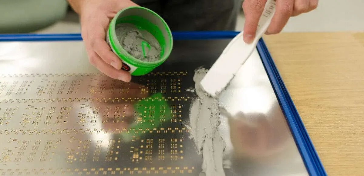
Solder paste inspection, or SPI, is a quality control step in the surface mount technology (SMT) process of PCB assembly. During PCB manufacturing, solder paste—a mixture of tiny solder particles and flux—is applied to the board’s pads to create connections between components and the PCB. If the solder paste isn’t applied correctly, it can lead to poor connections, component misalignment, or even complete failure of the final product.
SPI uses specialized machines to inspect the solder paste deposits right after they’re printed onto the PCB. It checks for issues like insufficient or excessive solder paste volume, incorrect height, uneven area coverage, or misalignment. By catching these problems early, SPI reduces the risk of defects during the reflow soldering process, saving time and money. In fact, studies suggest that up to 70% of soldering defects originate from improper solder paste application, making SPI a vital checkpoint.
How Does Solder Paste Inspection Work?
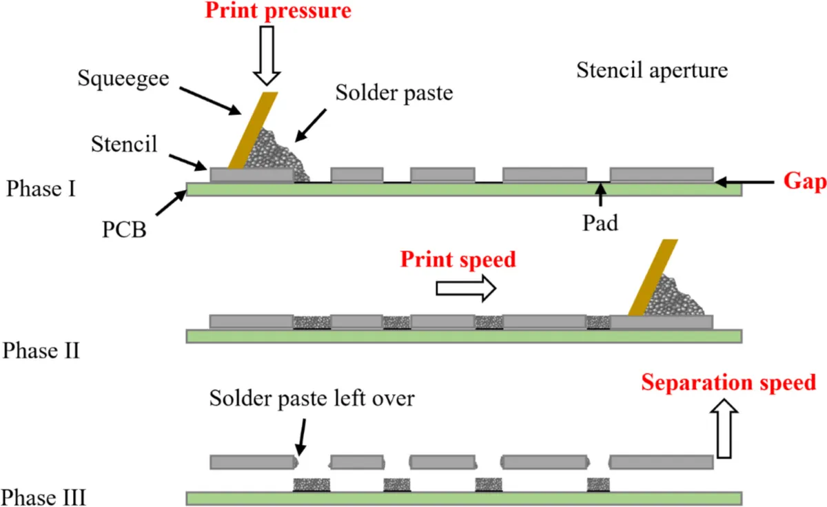
The SPI process typically happens right after the solder paste is printed onto the PCB using a stencil. Specialized SPI machines use advanced imaging technology to analyze the paste deposits. These machines capture detailed data about the solder paste and compare it against predefined standards to ensure quality.
Traditional 2D SPI systems rely on cameras to take flat images of the solder paste, which can detect basic issues like missing paste or misalignment. However, modern 3D SPI systems take this a step further. They use laser or structured light technology to create a three-dimensional view of the solder paste deposits. This allows for precise measurements of key parameters like solder paste volume, height, and area, providing a more accurate assessment of quality.
For example, a 3D SPI machine might measure that a solder paste deposit has a volume of 120 cubic micrometers, a height of 150 micrometers, and an area coverage of 90% of the pad. If any of these values fall outside acceptable ranges (e.g., a volume below 100 cubic micrometers), the system flags it as a potential defect. This level of detail helps manufacturers address issues before they escalate.

Key Parameters in Solder Paste Inspection
SPI focuses on several critical metrics to ensure the solder paste is applied correctly. Let's break down each parameter and why it matters in PCB manufacturing.
1. Solder Paste Volume
Solder paste volume refers to the total amount of paste deposited on each pad. Too little volume can lead to weak solder joints, while too much can cause bridging—where excess solder connects adjacent pads and creates a short circuit. 3D SPI systems measure solder paste volume in cubic micrometers to ensure it falls within a target range, often between 100 and 150 cubic micrometers for standard SMT pads. Maintaining the correct volume is crucial for reliable electrical connections.
2. Solder Paste Height
Solder paste height is the vertical thickness of the paste deposit, typically measured in micrometers. A height that’s too low (e.g., below 120 micrometers) might not provide enough material for a strong bond, while excessive height (e.g., above 180 micrometers) can lead to uneven soldering. SPI ensures the height is consistent across the board, often targeting a range of 130-160 micrometers for most applications.
3. Solder Paste Area
The solder paste area indicates how much of the pad is covered by paste. Ideally, the paste should cover 90-100% of the pad’s surface. If the area coverage drops below 80%, it could result in insufficient contact with the component lead, leading to poor soldering. 3D SPI systems provide precise area measurements to catch any gaps or uneven distribution early.
4. Solder Paste Alignment
Alignment refers to how accurately the solder paste is positioned on the pad. Misalignment—where the paste is offset by more than 25 micrometers—can cause components to shift during reflow soldering, leading to defective connections. SPI machines use high-resolution imaging to detect even slight misalignments and ensure the paste is centered on each pad.
Common Solder Paste Defects and How SPI Detects Them
Even with advanced printing techniques, solder paste application can go wrong. SPI is designed to catch these issues before they become bigger problems. Here are some common solder paste defects and how SPI helps identify them.
1. Insufficient Solder Paste
When there’s not enough solder paste on a pad, it can lead to weak or incomplete solder joints. This often happens due to stencil clogging or uneven pressure during printing. SPI detects insufficient solder paste by measuring low volume (e.g., below 100 cubic micrometers) or reduced area coverage (e.g., less than 80%).
2. Excessive Solder Paste
Too much solder paste can cause solder bridging or tombstoning, where components lift off the board during reflow. SPI identifies excessive paste by flagging high volume (e.g., above 150 cubic micrometers) or height (e.g., over 180 micrometers) values that exceed the acceptable range.
3. Solder Paste Bridging
Bridging occurs when solder paste connects two adjacent pads, often due to overprinting or misalignment. This defect can create short circuits in the final product. SPI systems spot bridging by detecting abnormal area coverage or paste deposits that extend beyond the pad boundaries.
4. Misaligned Solder Paste
If the solder paste isn’t centered on the pad, components may not align properly during placement. SPI catches misalignment by comparing the paste’s position to the pad’s center, flagging offsets greater than 25 micrometers.
5. Uneven Solder Paste Distribution
Uneven distribution—where paste is thicker in some areas than others—can lead to inconsistent soldering. 3D SPI technology maps the height and area of each deposit to identify variations that could affect quality.
The Advantages of 3D SPI in PCB Manufacturing
While 2D SPI systems can detect basic issues, 3D SPI offers a higher level of precision and reliability. Here’s why 3D SPI is becoming the standard in modern PCB manufacturing:
- Accurate Measurements: 3D SPI provides detailed data on solder paste volume, height, and area, allowing for tighter control over the process. For instance, it can detect height variations as small as 5 micrometers.
- Early Defect Detection: By catching issues before reflow soldering, 3D SPI reduces rework costs by up to 50% in some cases, as defects are fixed before components are placed.
- Improved Yield: With precise inspections, manufacturers can achieve higher first-pass yields, often exceeding 95%, leading to better overall efficiency.
- Support for Miniaturization: As PCBs become smaller and components denser, 3D SPI ensures accuracy for fine-pitch components with pad sizes as small as 0.3 mm.
Many advanced manufacturing facilities now rely on 3D SPI to meet the strict quality demands of industries like automotive, aerospace, and consumer electronics.
Best Practices for Effective Solder Paste Inspection
To get the most out of SPI, manufacturers should follow these best practices:
- Calibrate Equipment Regularly: Ensure SPI machines are calibrated to maintain accuracy in measurements like solder paste height and volume. A deviation of just 10 micrometers can affect results.
- Use High-Quality Stencils: A well-designed stencil with clean apertures prevents issues like insufficient paste or bridging. Regular cleaning after every 5-10 prints is recommended.
- Set Clear Standards: Define acceptable ranges for solder paste volume (e.g., 100-150 cubic micrometers), height (e.g., 130-160 micrometers), and alignment (e.g., within 25 micrometers) based on your project’s needs.
- Monitor Process Trends: Use SPI data to track trends over time, such as recurring low-volume deposits, to identify and fix root causes like stencil wear or printer settings.
- Train Operators: Equip your team with the skills to interpret SPI data and make quick adjustments to the printing process when defects are flagged.

Challenges in Solder Paste Inspection and How to Overcome Them
While SPI is a powerful tool, it’s not without challenges. One common issue is false positives, where the system flags a deposit as defective even though it’s acceptable. This can happen due to lighting conditions or surface reflections on the PCB. To minimize false positives, manufacturers can adjust the SPI machine’s sensitivity settings and ensure consistent lighting during inspections.
Another challenge is inspecting complex PCB designs with varying pad sizes and shapes. For example, a board with both large power pads and tiny 0.3 mm fine-pitch pads may require different inspection parameters. Using customizable 3D SPI software that allows for pad-specific settings can help address this issue.
Finally, the initial cost of SPI equipment can be high, often ranging from $50,000 to $150,000 for advanced 3D systems. However, the long-term savings from reduced rework and higher yields—sometimes improving by 10-20%—often justify the investment.
The Future of SPI in PCB Manufacturing
As PCB designs become more complex and components continue to shrink, the role of SPI will only grow. Emerging technologies like artificial intelligence (AI) and machine learning are being integrated into SPI systems to predict defects before they occur. For instance, AI can analyze historical SPI data to identify patterns that lead to low solder paste volume, allowing for proactive adjustments.
Additionally, the push for Industry 4.0 and smart manufacturing means SPI machines are becoming more connected. They can communicate with other equipment on the production line, such as solder paste printers, to automatically adjust settings in real-time. This level of automation could reduce defect rates to below 1% in the near future.
Conclusion: Why SPI is Essential for Quality PCB Manufacturing
Solder Paste Inspection is a cornerstone of quality control in PCB manufacturing. By meticulously checking solder paste volume, height, area, and alignment, SPI ensures that solder joints are reliable and defects are minimized. With the precision of 3D SPI technology, manufacturers can catch issues early, improve yields, and meet the stringent demands of modern electronics.
At ALLPCB, we understand the importance of quality at every stage of PCB assembly. Our commitment to advanced inspection processes like SPI helps deliver flawless boards for your projects. Whether you’re working on consumer gadgets or industrial systems, integrating SPI into your manufacturing process is a step toward consistent, high-quality results.