 ALLPCB


Printed Circuit Board (PCB) assembly is a complex process where precision is everything. Even small defects can lead to costly delays, unreliable products, and frustrated engineers. At ALLPCB, we understand the challenges you face in delivering high-quality PCBs on time. That's why we've put together this guide to help you reduce defects in your PCB assembly lines. Whether you're refining your design process or optimizing production, these strategies will help you achieve better results.
In this blog, we'll walk you through practical steps to minimize errors, backed by specific examples and data. From design tips to advanced manufacturing techniques, you'll find actionable advice to improve your assembly process. Let's get started.
Recommended Reading: Troubleshooting Common Defects in Batch Assembled PCBs
Understanding Common PCB Assembly Defects
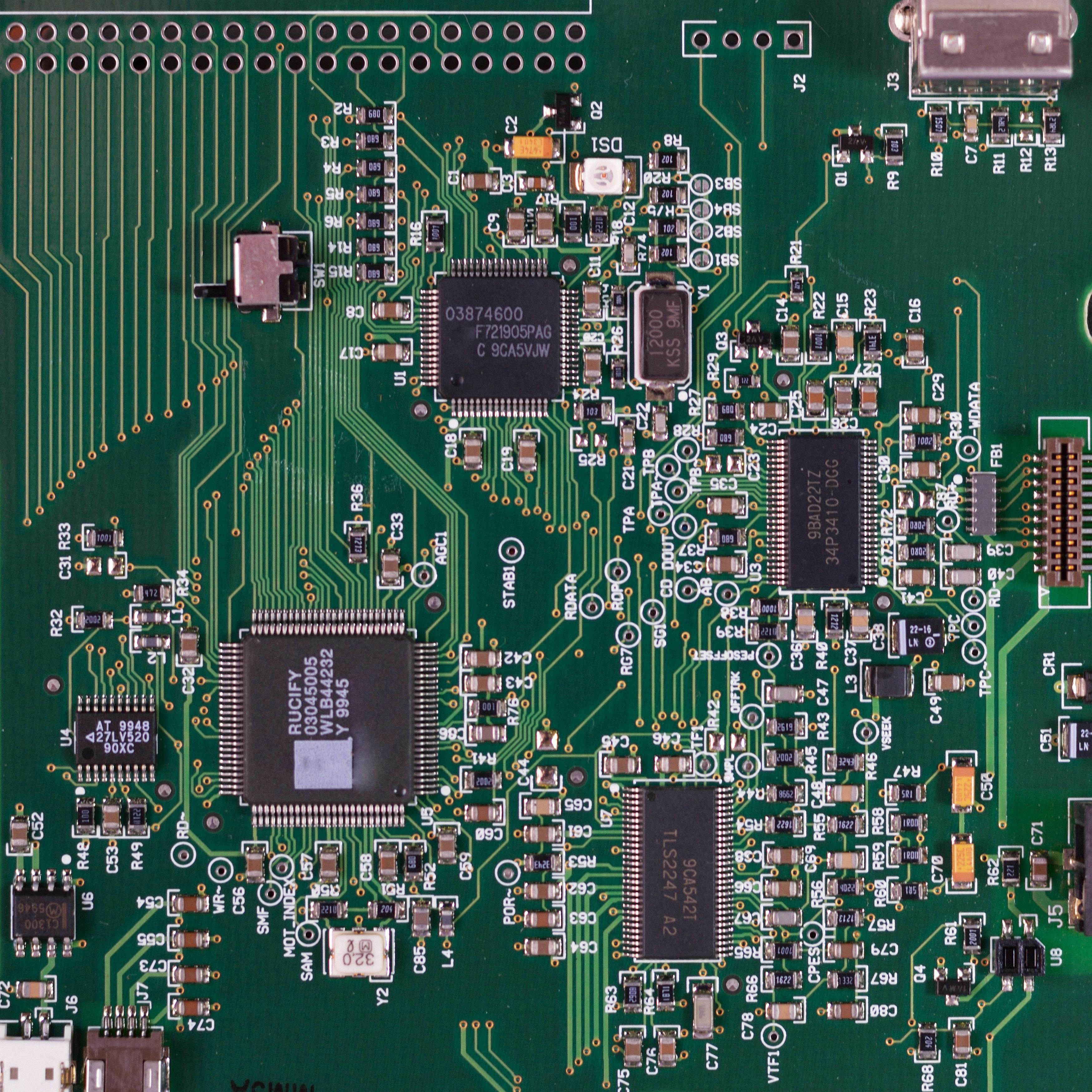
To reduce defects, you first need to know what you're up against. PCB assembly defects can pop up at any stage - design, component placement, soldering, or testing. Here are some of the most common issues engineers encounter:
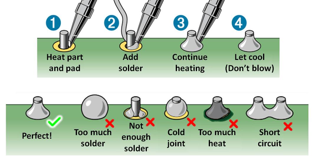
- Soldering Defects: Cold solder joints, solder bridges, or insufficient solder can weaken connections or cause shorts.
- Component Misplacement: Parts placed incorrectly or misaligned can disrupt functionality.
- Tombstoning: When one side of a component lifts during soldering, often due to uneven heating.
- Solder Mask Problems: Missing or misapplied solder masks can expose areas to unwanted solder or contamination.
- Testing Gaps: Skipping thorough testing lets defects slip through to the final product.
These issues can compromise your PCB's performance. By targeting their root causes, you can cut down on rework and boost reliability. Let's explore how.
Designing for Manufacturability (DFM)
A solid design sets the stage for a defect-free assembly. Design for Manufacturability (DFM) is about creating PCBs that are easy to produce with minimal errors. Here's how to apply DFM principles:
- Component Spacing: Leave enough room between parts for automated tools. A minimum clearance of 0.5mm prevents pick-and-place machines from bumping into neighboring components.
- Trace Width and Spacing: Keep traces at least 0.2mm apart for standard boards to avoid shorts. Wider traces (e.g., 0.3mm) also handle current better and reduce soldering risks.
- Thermal Balance: Design your layout to spread heat evenly during soldering. Uneven heating can lift components, causing tombstoning.
- Solder Mask Coverage: Always include a solder mask to shield against bridges and debris. It's a small step that pays off big.
Focusing on DFM reduces assembly headaches down the line. It's a proactive way to catch defects before they start.
Optimizing the Soldering Process
Soldering is where many defects take shape. A well-controlled soldering process can make all the difference. Here's how to get it right:
- Temperature Precision: Match your soldering temp to your materials. Lead-free solder, for instance, needs 240°C to 260°C in a reflow oven.
- Even Heating: Use multi-zone reflow ovens to distribute heat consistently. This prevents tombstoning and ensures solid joints.
- Solder Paste Application: Apply paste evenly with a stencil matched to your pad sizes. Too much paste leads to bridges; too little starves joints.
- Early Inspection: Add automated optical inspection (AOI) post-soldering. AOI spots defects like solder bridges with over 95% accuracy.
A dialed-in soldering process cuts defects and boosts PCB reliability. It's worth the effort to fine-tune this step.
Implementing Rigorous Testing Procedures
Testing catches defects before they become bigger problems. A strong testing plan covers both functionality and durability. Here's how to build one:
- In-Circuit Testing (ICT): ICT checks soldering, placement, and connections. It can detect an open circuit or short in seconds.
- Functional Testing: Verify the PCB does its job. For a Wi-Fi module, test signal strength at 2.4GHz to confirm performance.
- Environmental Stress: Run tests like thermal cycling (-40°C to 85°C) to expose weak solder joints or material flaws.
- Test Points: Add accessible test points to your design. One per net ensures you can probe without hassle.
Thorough testing means fewer surprises later. It's your safety net for quality control.
Ensuring Component Quality and Placement Accuracy
Defects often trace back to components - either their quality or how they're placed. Here's how to keep this under control:
- Accurate BOM: Double-check your Bill of Materials for correct part numbers. A wrong resistor value (e.g., 10kΩ instead of 1kΩ) can throw everything off.
- Placement Verification: Use vision systems to confirm components are spot-on. Aim for a tolerance of ±0.1mm for precision.
- Trusted Suppliers: Source parts from reliable vendors to dodge counterfeits. Fake chips can fail under load, ruining your board.
- Proper Storage: Keep components dry and ESD-safe. Moisture-sensitive parts need humidity below 5% to stay defect-free.
High-quality components, placed accurately, are the backbone of a solid PCB.
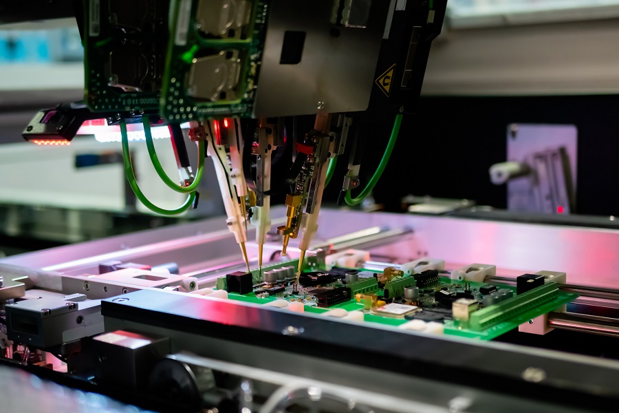
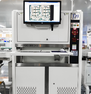
Leveraging Advanced Manufacturing Technologies
Technology can take your defect reduction to the next level. These tools boost precision and catch issues early:
- Automated Optical Inspection (AOI): AOI scans boards at up to 100cm² per second, flagging soldering or placement errors.
- X-Ray Inspection: For hidden joints (like BGAs), X-rays reveal voids or misalignments that AOI can't see.
- Robotic Soldering: Robots apply solder consistently, cutting human error and ensuring uniform joints.
- Data Insights: Analyze inspection data to spot patterns. If soldering temps drift by 5°C, you'll know to adjust.
These technologies streamline your process and keep defects low. They're an investment in quality.
Partnering with a Reliable PCB Manufacturer
Even with the best in-house efforts, a skilled manufacturing partner can elevate your results. At ALLPCB, we bring advanced tools and expertise to the table. Our quick-turn prototyping gets your designs built fast, while our state-of-the-art facilities ensure precision assembly. With global logistics, we deliver defect-free PCBs wherever you are. Whether it's a one-off prototype or a full production run, we're here to help you succeed.
Conclusion
Reducing defects in PCB assembly lines comes down to smart design, tight process control, and robust testing. By embracing DFM, perfecting soldering, verifying components, and using cutting-edge tech, you can build PCBs that perform flawlessly. At ALLPCB, we're proud to support engineers with the tools and services to make that happen. Follow these steps, and you'll see fewer defects - and happier customers.


