 ALLPCB


In the fast-evolving world of electronics, the demand for smaller, more powerful devices has never been greater. High-density interconnect PCB assembly (HDI PCB assembly) is at the heart of this revolution, enabling the creation of miniaturized electronic devices without sacrificing performance. If you're looking to master high-density rigid board assembly and learn techniques for miniaturization, you've come to the right place. This guide will walk you through the essentials of HDI PCB design rules, fine-pitch component placement, microvia technology, and more, offering practical insights for engineers and designers.
At ALLPCB, we understand the challenges of designing and assembling compact, high-performance boards. In this blog, we'll dive deep into the strategies and techniques that can help you achieve miniaturization while maintaining reliability and efficiency. Let's explore the world of high-density interconnect PCB assembly and uncover the tools and methods that drive innovation in modern electronics.
What is High-Density Interconnect PCB Assembly?
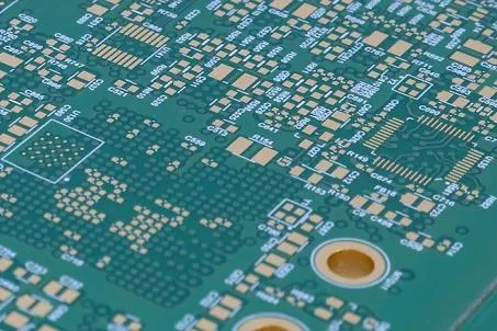
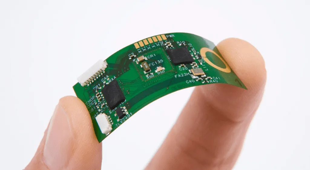
High-density interconnect PCB assembly, often referred to as HDI PCB assembly, is a specialized manufacturing process that allows for a higher number of connections in a smaller space. Unlike traditional printed circuit boards, HDI boards use advanced techniques like microvias, blind vias, and buried vias to pack more components into a compact area. This makes them ideal for miniaturized electronic devices such as smartphones, wearables, medical equipment, and automotive systems.
The primary goal of HDI PCB assembly is to achieve miniaturization while ensuring signal integrity and thermal management. By utilizing finer lines, smaller vias, and tighter spacing, these boards can support complex designs with high-speed signals, often exceeding 5 GHz in advanced applications. For engineers, understanding HDI technology is crucial for meeting the demands of modern electronics where space is at a premium.
Key Techniques for High-Density Rigid Board Assembly
Creating a high-density rigid board requires precision and a deep understanding of advanced assembly techniques. Below, we’ll explore the core methods that enable miniaturization and ensure the performance of HDI PCBs.
1. Fine-Pitch Component Placement
Fine-pitch component placement is a cornerstone of high-density interconnect PCB assembly. This technique involves placing components with very small lead spacing, often less than 0.5 mm, to maximize the use of available board space. It is commonly used for ball grid arrays (BGAs), chip-scale packages (CSPs), and other compact components.
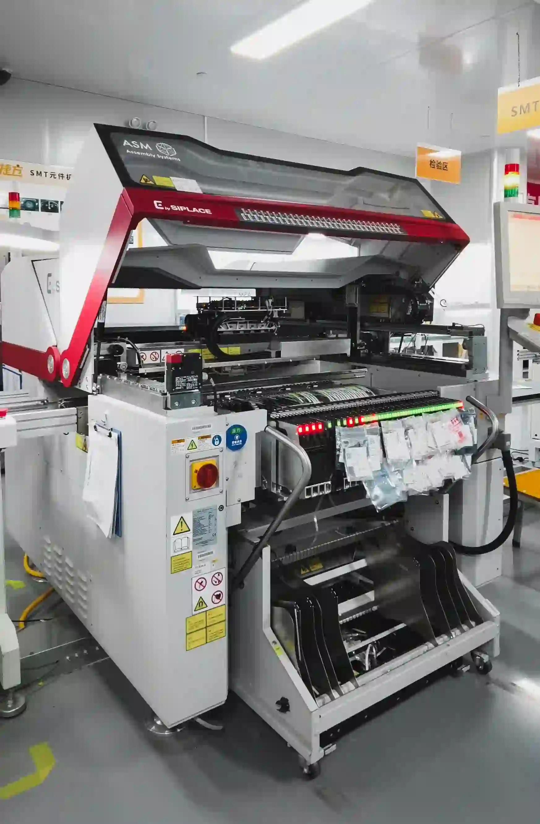
To achieve successful fine-pitch placement, automated pick-and-place machines are essential. These machines can position components with accuracies down to 0.01 mm, ensuring alignment even with the smallest footprints. Additionally, designers must follow strict HDI PCB design rules, such as maintaining a minimum pad-to-pad clearance of 0.1 mm, to prevent soldering defects like bridging or tombstoning.
Practical Tip: Use high-resolution optical inspection systems during assembly to verify the placement of fine-pitch components. This reduces the risk of misalignment and ensures reliable connections.
2. Leveraging Microvia Technology
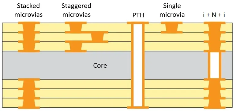
Microvia technology is a game-changer for HDI PCB assembly. Microvias are tiny holes, typically less than 0.15 mm in diameter, that connect different layers of a PCB. Unlike traditional through-hole vias, microvias take up less space and allow for higher routing density, making them perfect for miniaturized electronic devices.
There are two main types of microvias used in HDI designs: blind vias, which connect an outer layer to an inner layer, and buried vias, which connect inner layers without reaching the surface. Laser drilling is often used to create these microvias with precision, achieving aspect ratios as high as 1:1. This technology not only saves space but also improves signal integrity by reducing parasitic capacitance and inductance.
Practical Tip: When designing with microvias, ensure that the stack-up configuration supports a minimum via pad diameter of 0.25 mm to maintain manufacturability. Collaborate with your PCB manufacturer to confirm drilling capabilities for your specific design.
3. Adhering to HDI PCB Design Rules
Designing an HDI PCB requires strict adherence to specific design rules to ensure functionality and manufacturability. These HDI PCB design rules cover aspects like trace width, spacing, via sizes, and layer stack-up configurations. For instance, trace widths in HDI boards are often reduced to 0.075 mm or less, and spacing between traces can be as tight as 0.05 mm to accommodate high-density routing.
Signal integrity is another critical consideration. High-speed signals, often operating at frequencies above 1 GHz, require controlled impedance, typically around 50 ohms for single-ended lines or 100 ohms for differential pairs. Designers must use simulation tools to predict and mitigate issues like crosstalk and signal reflection in densely packed layouts.
Practical Tip: Incorporate ground planes and proper shielding in your design to minimize electromagnetic interference (EMI) in high-density layouts. This is especially important for miniaturized electronic devices where components are closely spaced.
Strategies for Miniaturization in HDI PCB Assembly
Miniaturization is the ultimate goal of high-density interconnect PCB assembly. It’s not just about making devices smaller; it’s about maintaining or even enhancing performance in a reduced footprint. Here are some proven strategies to achieve miniaturization in your designs.
1. Optimize Layer Stack-Up for Compact Designs
The layer stack-up of an HDI PCB plays a vital role in miniaturization. By using multiple layers—often 8 or more in advanced designs—engineers can route complex circuits in a smaller area. A typical HDI stack-up might include a combination of microvias and buried vias to connect layers without wasting surface space.
For example, a 10-layer HDI board for a wearable device might use a 2+N+2 configuration, where "N" represents the core layers, and the "2" refers to build-up layers on either side. This approach allows for denser routing while keeping the board thickness under 1.6 mm, a common requirement for compact electronics.
Practical Tip: Work closely with your PCB fabricator to balance the number of layers with cost and manufacturability. Over-specifying layers can increase production costs without significant performance gains.
2. Use Advanced Materials for Higher Density
Material selection is critical for high-density rigid board assembly. Traditional FR-4 materials may not suffice for HDI designs due to their limitations in thermal performance and dielectric properties. Instead, high-performance materials like polyimide or high-Tg laminates are often used to support finer traces and better heat dissipation.
These materials can maintain stability at temperatures above 150°C and support dielectric constants as low as 3.5, which is essential for high-speed signal transmission in miniaturized electronic devices. Additionally, thinner substrates, often below 0.2 mm per layer, help reduce the overall board thickness.
3. Integrate Embedded Components
Embedding components within the PCB substrate is an innovative strategy for miniaturization. By placing passive components like resistors and capacitors inside the board layers, designers can free up valuable surface space for active components or additional routing. This technique is particularly useful for applications like medical implants or IoT devices, where size constraints are extreme.
Embedded components also improve signal integrity by reducing trace lengths and minimizing parasitic effects. However, this approach requires precise manufacturing capabilities and thorough testing to ensure reliability.
Practical Tip: Start with embedding simple passives before moving to more complex components. Ensure that your design software supports embedded component modeling for accurate simulations.
Challenges in High-Density Interconnect PCB Assembly
While HDI PCB assembly offers incredible benefits for miniaturization, it comes with its share of challenges. Understanding these obstacles can help you design and assemble boards more effectively.
1. Thermal Management in Compact Designs
As components are packed closer together in miniaturized electronic devices, heat dissipation becomes a significant concern. High-density designs can generate substantial heat, especially in power-intensive applications like 5G modules or automotive control units. Without proper thermal management, this heat can degrade performance or cause component failure.
Solutions include using thermal vias to transfer heat to outer layers and incorporating heat sinks or metal cores in the PCB design. For instance, thermal vias with a diameter of 0.3 mm can effectively channel heat away from critical components, maintaining operating temperatures below 85°C.
2. Manufacturing Complexity and Cost
HDI PCB assembly is inherently more complex than traditional PCB manufacturing. The use of microvias, fine-pitch components, and multiple layers increases production time and cost. Laser drilling for microvias, for example, requires specialized equipment and expertise, which can drive up expenses.
To mitigate costs, focus on design for manufacturability (DFM) principles. Optimize your layout to minimize the number of microvias and build-up layers while still meeting performance requirements. Partnering with an experienced PCB manufacturer can also help streamline the process.
Conclusion: Achieving Miniaturization with HDI PCB Assembly
Mastering high-density rigid board assembly is key to unlocking the potential of miniaturized electronic devices. By leveraging techniques like fine-pitch component placement, microvia technology, and strict adherence to HDI PCB design rules, engineers can create compact, high-performance designs for a wide range of applications. At ALLPCB, we’re committed to supporting your journey toward miniaturization with advanced manufacturing capabilities and expert guidance.
Whether you’re designing for consumer electronics, medical devices, or automotive systems, the strategies outlined in this guide can help you overcome the challenges of high-density interconnect PCB assembly. Embrace these techniques to stay ahead in the race for smaller, smarter, and more efficient electronics.


