 ALLPCB


If you're looking for a reliable double-sided PCB component placement guide, you're in the right place. Double-sided PCB assembly can be a game-changer for compact, high-performance designs, but it comes with unique challenges. In this comprehensive guide, we'll cover double-sided PCB design rules, SMT component placement best practices, and reflow soldering challenges for double-sided boards. Whether you're a beginner or an experienced engineer, you'll find actionable tips and detailed insights to optimize your designs for manufacturing success.
Introduction to Double-Sided PCB Assembly
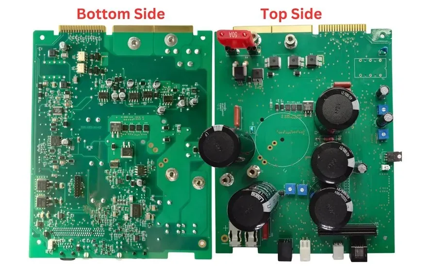
Double-sided PCBs are a popular choice in modern electronics because they allow components to be placed on both sides of the board, effectively doubling the available space for circuitry. This design is ideal for compact devices like smartphones, IoT gadgets, and medical equipment, where space is at a premium. However, with great flexibility comes greater complexity. Proper component placement and adherence to design rules are critical to avoid issues like signal interference, thermal imbalance, and soldering defects during assembly.
In this guide, we'll walk through the essentials of mastering double-sided PCB assembly. From understanding the basics to tackling advanced challenges like reflow soldering, you'll gain the knowledge needed to create efficient and reliable designs. Let's dive into the key aspects of double-sided PCB component placement and design.
Why Double-Sided PCB Assembly Matters
Double-sided PCBs offer significant advantages over single-sided boards. They provide more room for components and traces, enabling denser and more complex circuits without increasing the board's footprint. This makes them ideal for applications where size and weight are critical factors. However, the added complexity of working on both sides of the board introduces challenges in design, assembly, and manufacturing.
Poor component placement can lead to issues like crosstalk between signals, uneven heat distribution, and difficulties during soldering. By mastering double-sided PCB design rules and placement strategies, you can minimize these risks and ensure your board performs as intended. Let's explore the foundational principles that guide successful double-sided PCB assembly.
Key Double-Sided PCB Design Rules for Success
Designing a double-sided PCB requires careful planning to ensure functionality and manufacturability. Here are some essential design rules to follow:
- Layer Assignment: Assign specific functions to each side of the board. For example, place power and ground planes on one side to minimize noise, while placing high-speed signal components on the other side to reduce interference. This helps manage signal integrity, especially for frequencies above 100 MHz.
- Via Placement: Use vias strategically to connect traces between the top and bottom layers. Avoid placing vias under components, as this can interfere with soldering. Keep via density below 50 vias per square inch in high-component areas to prevent manufacturing issues.
- Clearance and Spacing: Maintain adequate spacing between components and traces to avoid short circuits. A minimum clearance of 0.2 mm (8 mils) between traces and 0.5 mm (20 mils) between components is a good starting point for most designs.
- Thermal Balance: Distribute heat-generating components evenly across both sides to prevent warping during reflow soldering. For example, if a power IC dissipates 2W of heat, avoid clustering other heat sources nearby on the same side.
By adhering to these double-sided PCB design rules, you create a foundation for a board that is easier to assemble and less prone to errors during manufacturing.
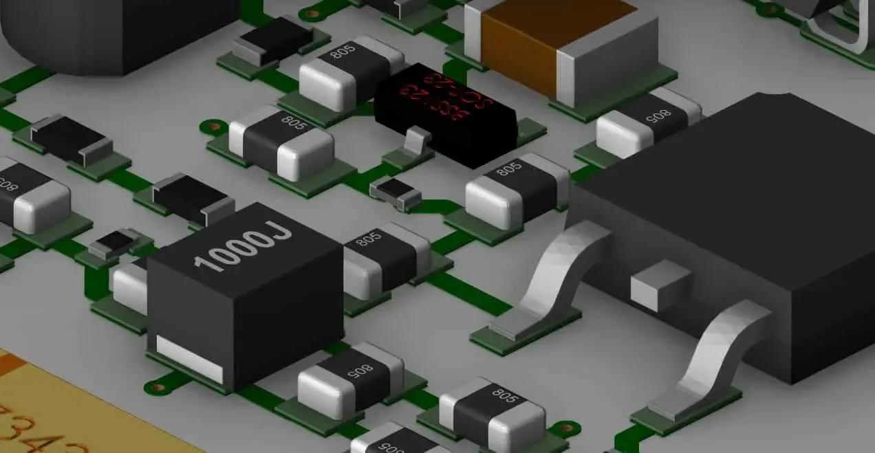
SMT Component Placement Best Practices for Double-Sided PCBs
Surface Mount Technology (SMT) is the dominant method for assembling double-sided PCBs due to its efficiency and compatibility with automated processes. However, placing SMT components on both sides of a board requires precision to ensure reliability. Here are some SMT component placement best practices tailored for double-sided designs:
1. Prioritize Component Weight and Size
Larger and heavier components, such as connectors and capacitors, should typically be placed on the bottom side of the PCB during assembly. This prevents them from falling off during the second reflow soldering pass when the board is flipped. For instance, components weighing over 5 grams are often better suited for the bottom side to ensure stability.
2. Group Components by Function
Place related components close together to minimize trace lengths and reduce signal delay. For high-speed designs, keep critical components like microcontrollers and memory chips within 10 mm of each other to maintain signal integrity at speeds up to 500 MHz.
3. Avoid Overlapping High-Density Areas
Distribute components evenly to avoid overcrowding on one side. Overlapping high-density areas can lead to heat concentration and soldering defects. Aim for a balanced layout where neither side exceeds 70% component coverage.
4. Consider Pick-and-Place Machine Limitations
Align components in a grid pattern with consistent orientation (e.g., 0° or 90°) to simplify automated assembly. This reduces errors during placement and ensures compatibility with standard pick-and-place machines, which often have angular placement constraints.
Following these SMT component placement best practices will help you achieve a design that is both functional and manufacturable, minimizing risks during the assembly process.
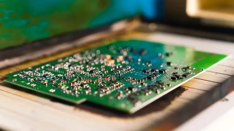
Reflow Soldering Challenges for Double-Sided PCBs
Reflow soldering is a critical step in double-sided PCB assembly, but it presents unique challenges due to the need to solder components on both sides. Understanding and addressing these reflow soldering challenges for double-sided boards is essential for a successful outcome.
1. Component Displacement During Second Reflow
During the second reflow pass (when the board is flipped), components on the bottom side can shift or fall off due to gravity and melted solder. To mitigate this, use high-temperature solder paste for the first side and ensure heavier components (over 5 grams) are secured with adhesive if necessary.
2. Thermal Imbalance
Uneven heat distribution during reflow can cause the board to warp, leading to poor solder joints. For example, if one side has a large copper pour acting as a heat sink, it may cool faster than the other side. To counter this, design for thermal symmetry by balancing copper areas and component density. Limit copper pour differences to less than 20% between sides.
3. Solder Joint Reliability
Double-sided boards often require multiple reflow cycles, which can stress solder joints and lead to defects like tombstoning, where small components stand upright due to uneven heating. Use a reflow profile with a gradual ramp-up (1-2°C per second) to a peak temperature of 245°C for lead-free solder to minimize thermal shock.
4. Flux Residue and Cleaning
Flux residue trapped between components on densely packed double-sided boards can cause corrosion over time. Opt for no-clean flux when possible, or ensure thorough cleaning with isopropyl alcohol post-reflow to remove residues, especially in areas with less than 0.3 mm clearance.
By anticipating these reflow soldering challenges for double-sided PCBs and implementing the suggested solutions, you can improve the reliability and quality of your assembled boards.
Advanced Tips for Optimizing Double-Sided PCB Assembly
Beyond the basics, there are advanced strategies to further enhance your double-sided PCB designs. These tips can help you tackle complex projects with confidence.
- Signal Integrity Analysis: For high-speed designs, use simulation tools to analyze signal integrity. Maintain controlled impedance (e.g., 50 ohms for RF signals) by adjusting trace widths and layer spacing. A typical trace width of 0.15 mm on a 1.6 mm thick board can achieve this for many applications.
- Design for Testability: Include test points on both sides of the board for in-circuit testing. Place them at least 2 mm apart to ensure probe access during debugging.
- Panelization for Manufacturing: Design your PCB with panelization in mind to optimize assembly efficiency. Leave a minimum of 5 mm between individual boards in a panel to allow for clean separation after assembly.
These advanced techniques can elevate your double-sided PCB assembly process, ensuring better performance and manufacturability for even the most demanding projects.
Common Mistakes to Avoid in Double-Sided PCB Component Placement
Even experienced designers can make errors when working with double-sided PCBs. Here are some common pitfalls to watch out for:
- Ignoring Thermal Distribution: Placing all heat-generating components on one side can lead to board warping. Spread out components like voltage regulators and power transistors to balance heat dissipation.
- Overlooking Component Height: Tall components on the bottom side can interfere with automated assembly or enclosure fitting. Keep bottom-side components under 3 mm in height when possible.
- Neglecting Solder Mask Expansion: Insufficient solder mask expansion (e.g., less than 0.05 mm around pads) can lead to solder bridging. Ensure proper expansion to expose enough copper for reliable joints.
Avoiding these mistakes will save you time and resources during the design and assembly stages, leading to a smoother production process.
Conclusion: Achieving Excellence in Double-Sided PCB Assembly
Mastering double-sided PCB assembly is a valuable skill for any electronics designer. By following this double-sided PCB component placement guide, adhering to double-sided PCB design rules, implementing SMT component placement best practices, and addressing reflow soldering challenges for double-sided boards, you can create high-quality, reliable designs that meet the demands of modern applications.
Start with a solid foundation of design rules, prioritize balanced component placement, and anticipate manufacturing challenges like thermal imbalance and component displacement. With careful planning and attention to detail, your double-sided PCB projects will achieve optimal performance and durability.


