ALLPCB


Are you looking to turn your electronic ideas into a functional rigid board? The process of rigid board assembly—from creating a schematic to soldering components and testing the final product—can seem daunting. However, with a clear roadmap, it becomes manageable and even exciting. In this comprehensive guide, we’ll walk you through every stage of the PCB design workflow, including component selection, PCB layout techniques, soldering techniques for beginners, and testing assembled PCBs. Whether you're a hobbyist or a budding engineer, this step-by-step tutorial will help you build a reliable printed circuit board with confidence.
Introduction to Rigid Board Assembly
Rigid board assembly is the process of designing, manufacturing, and assembling a printed circuit board (PCB) that serves as the backbone of most electronic devices. Unlike flexible boards, rigid PCBs are made from solid materials like fiberglass, providing durability for applications in consumer electronics, industrial equipment, and more. Mastering this process involves several key steps, each requiring attention to detail and precision. Let’s dive into the complete PCB design workflow to help you create a functional and efficient board.
Step 1: Creating a Schematic – The Blueprint of Your PCB
The first step in any PCB design workflow is creating a schematic. Think of it as the blueprint for your circuit. A schematic is a diagram that shows how components connect electrically, without worrying about their physical placement on the board. This stage sets the foundation for the entire project.
Start by defining the purpose of your circuit. Are you building a simple LED circuit or a complex microcontroller system? List all the components you’ll need, such as resistors, capacitors, ICs, and connectors. Use design software to draw the schematic, ensuring every connection is accurate. Double-check for errors, as mistakes here can lead to costly redesigns later.
For example, if you're designing a power supply circuit, ensure that the voltage regulator is connected properly to handle input voltages (e.g., 12V) and output the desired voltage (e.g., 5V). Label each component with its value or part number to avoid confusion during component selection.
Step 2: Component Selection – Choosing the Right Parts
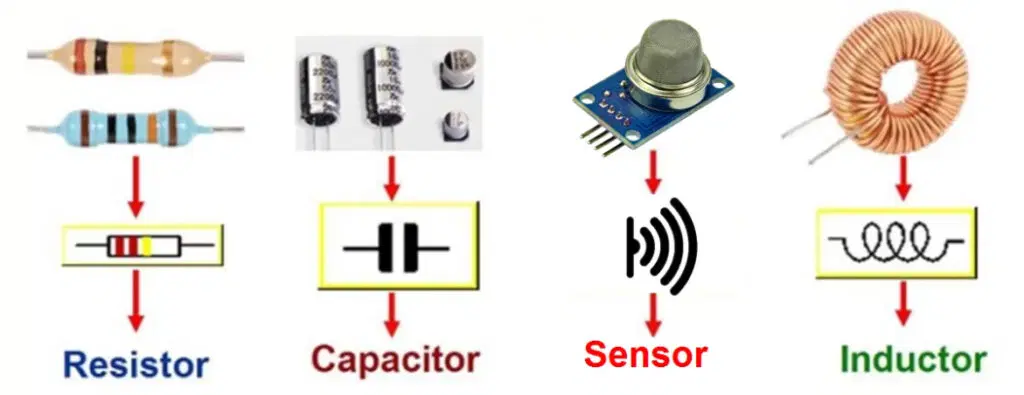
Once your schematic is ready, the next step in the PCB design workflow is component selection. Choosing the right components is critical to ensure your circuit functions as intended and fits within your budget and design constraints.
Consider factors like electrical specifications, size, availability, and cost. For instance, if you’re selecting a resistor for a current-limiting application in an LED circuit, calculate the required resistance using Ohm’s Law (V=IR). If your LED needs 20mA at 2V with a 5V supply, you’ll need a resistor of about 150 ohms (5V - 2V = 3V; 3V / 0.02A = 150Ω). Always choose components with a slightly higher tolerance for safety—opt for a 1/4W resistor instead of 1/8W if heat dissipation is a concern.
Also, prioritize components with standard footprints for easier assembly. Check datasheets for pin configurations and thermal requirements, especially for ICs or power components. If you're a beginner, start with through-hole components, as they are easier to solder than surface-mount devices (SMDs).
Step 3: PCB Layout Techniques – Designing for Functionality
With your schematic finalized and components selected, it’s time to design the physical layout of your PCB. This step, often called board layout, is where PCB layout techniques come into play. A well-designed layout minimizes noise, ensures signal integrity, and makes assembly easier.
Begin by placing components logically. Group related components together—for example, keep power supply components near the input connector to reduce trace lengths. Place high-speed components, like microcontrollers, close to their supporting capacitors to minimize interference. Maintain at least 10-15 mils (0.010-0.015 inches) of spacing between traces to prevent short circuits, especially for signals operating at high frequencies (e.g., above 100 MHz).
Pay attention to trace routing. Use wider traces (e.g., 20-30 mils) for power lines to handle higher currents, and narrower traces (e.g., 6-8 mils) for signal lines. Avoid sharp 90-degree angles in traces, as they can cause signal reflection; instead, use 45-degree angles or curves. For multilayer boards, dedicate one layer to ground to reduce electromagnetic interference (EMI).
Finally, add silkscreen labels for component placement and polarity. This makes assembly and debugging much easier, especially for beginners.
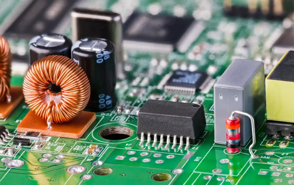
Step 4: Manufacturing the PCB – Bringing Your Design to Life
After completing the layout, export your design files (often in Gerber format) and send them for manufacturing. This step transforms your digital design into a physical rigid board. When choosing a manufacturing service, ensure they support your board specifications, such as layer count, material (e.g., FR-4), and thickness (typically 1.6mm for standard rigid boards).
Review the design rules check (DRC) in your software before submission to catch errors like overlapping traces or insufficient clearances. Most manufacturers offer a minimum trace width of 6 mils and spacing of 6 mils for standard processes, so ensure your design complies with these limits.
Once manufactured, inspect the bare board for defects like misaligned drill holes or broken traces before moving to assembly.
Step 5: Soldering Techniques for Beginners – Assembling Your Board
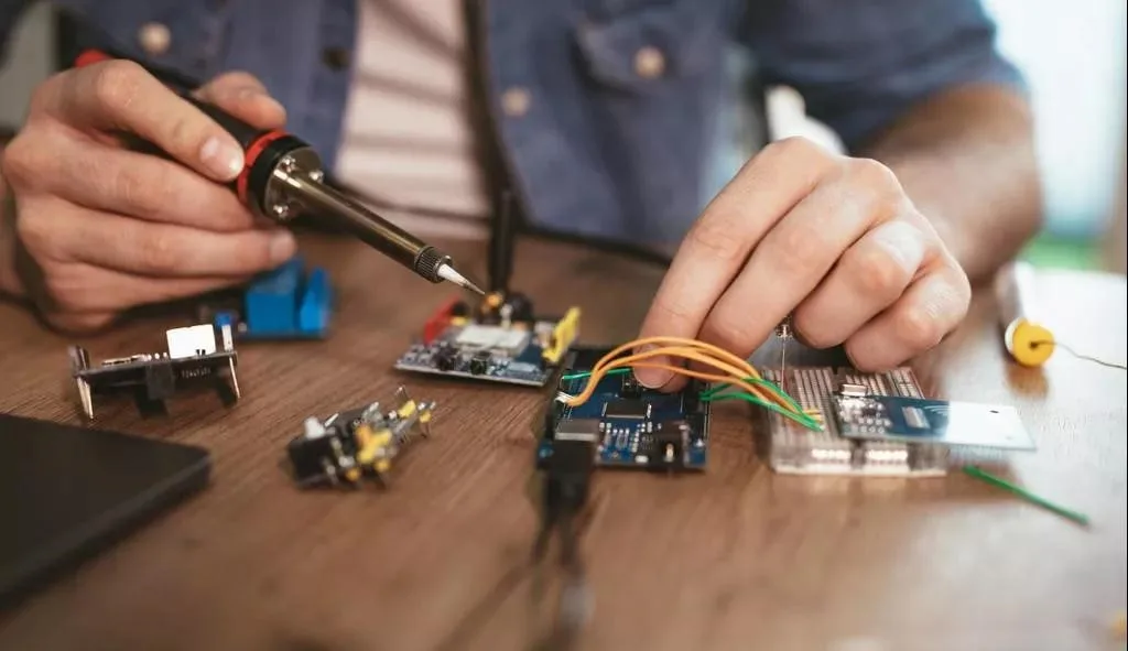
Now comes the hands-on part: assembling and soldering components onto your rigid board. For those new to this, mastering soldering techniques for beginners is essential to avoid damaging components or creating unreliable connections.
Start with the right tools: a soldering iron (25-40W for beginners), solder wire (60/40 tin-lead or lead-free), flux, and a desoldering wick for corrections. Work in a well-ventilated area and wear safety glasses. Set your soldering iron to around 300°C (572°F) for through-hole components and slightly lower (250-280°C) for SMDs to prevent overheating.
Begin by soldering smaller components like resistors and capacitors before moving to larger ones like connectors. Place the component in its designated spot, heat the pad and lead with the iron for 2-3 seconds, then apply solder until it flows smoothly around the joint. A good solder joint looks shiny and conical, not dull or blobby. Avoid excessive heat—limit contact to 5 seconds per joint to prevent damage.
For SMD components, use a small tip on your iron and apply solder paste if available. Align the component carefully, heat one pad, apply solder, then move to the other pads. Clean excess flux with isopropyl alcohol and a brush after soldering.
Step 6: Testing Assembled PCBs – Ensuring Functionality
After soldering, the final step is testing assembled PCBs to confirm everything works as designed. Testing prevents faulty boards from being deployed and helps identify issues early.
First, perform a visual inspection. Look for cold solder joints (dull or cracked connections), misplaced components, or burnt areas. Use a multimeter to check for continuity between power and ground—there should be no short circuits. Measure voltages at key points; for example, if your circuit outputs 5V, confirm this with your multimeter at the output pin.
Next, power up the board gradually. Use a current-limited power supply if possible to avoid damage from shorts. Observe for unusual behavior like overheating or smoke. Test individual functions—for a microcontroller board, upload a simple program to blink an LED and verify operation.
If issues arise, trace them back using your schematic. Common problems include reversed polarity on diodes or capacitors, incorrect component values, or broken traces. Fix these with desoldering tools and retest until the board functions correctly.
Common Mistakes to Avoid in Rigid Board Assembly
Even with careful planning, mistakes can happen during rigid board assembly. Here are some pitfalls to watch for:
- Schematic Errors: Missing connections or wrong component values can ruin a design. Always double-check before moving to layout.
- Poor Layout Choices: Overcrowding components or ignoring trace width can cause noise or heat issues. Follow PCB layout techniques for spacing and routing.
- Soldering Mishaps: Overheating components or creating cold joints can lead to failures. Practice soldering techniques for beginners on scrap boards first.
- Skipping Tests: Failing to test thoroughly can result in deploying a faulty board. Always prioritize testing assembled PCBs.
Tips for Success in Your PCB Design Workflow
To streamline your PCB design workflow and achieve better results, keep these tips in mind:
- Start with simple projects to build skills before tackling complex designs.
- Use design software with simulation features to test your schematic virtually before manufacturing.
- Keep a stock of common components to avoid delays during component selection.
- Document every step, from design to testing, for future reference or troubleshooting.
Conclusion: Mastering Rigid Board Assembly
Building a rigid PCB from schematic to soldering is a rewarding process that combines creativity and technical skill. By following this step-by-step guide, you’ve learned the essentials of the PCB design workflow, from creating a schematic and mastering component selection to applying effective PCB layout techniques. You’ve also gained insights into soldering techniques for beginners and the importance of testing assembled PCBs to ensure functionality.
Every project is a learning opportunity. As you gain experience, you’ll refine your skills and tackle more complex designs with ease. With the right approach and attention to detail, your electronic ideas can come to life on a reliable, well-assembled rigid board.