 ALLPCB


Designing a product that's both functional and cost-effective requires careful consideration of how it'll be assembled. Design for Assembly (DFA) is a methodology that streamlines the assembly process by reducing part counts, simplifying component designs, and minimizing assembly time. For engineers, implementing DFA principles early in the design phase can reduce manufacturing costs by up to 50% and improve product reliability. This blog post provides a comprehensive DFA checklist tailored for engineers, drawing from industry best practices to help you optimize your designs for efficient assembly.
Why DFA Matters for Engineers
DFA is a proactive approach that focuses on ease of assembly during the design phase, saving time and resources compared to fixing issues during production. By addressing assembly challenges early, engineers can reduce errors, lower labor costs, and accelerate time-to-market. For example, studies show that over 70% of a product's final cost is determined during the design stage, making DFA a critical tool for cost control. Whether you're designing consumer electronics, automotive components, or industrial equipment, adhering to DFA principles ensures your product is easier to assemble and more reliable in the field.
This checklist outlines actionable steps to integrate DFA into your workflow, ensuring your designs are optimized for manufacturability and assembly efficiency.
DFA Checklist for Engineers
1. Minimize Part Count
Reducing the number of parts is a cornerstone of DFA. Fewer parts mean fewer assembly steps, lower inventory costs, and reduced opportunities for defects. For each component, ask: 'Is this part necessary?' and 'Can its function be combined with another part?' For instance, combining a bracket and a housing into a single molded component can eliminate an assembly step and reduce material costs by 10-20%.
-
Actionable Tip: Perform a functional analysis to identify redundant parts. Use Boothroyd Dewhurst DFA guidelines to evaluate whether each component moves relative to others, requires a different material, or serves a unique function.
-
Example: In PCB design, replacing multiple discrete resistors with a single resistor array can reduce placement time by 15% during surface-mount technology (SMT) assembly.
2. Standardize Components
Using standardized components simplifies procurement, reduces costs, and enhances reliability. Custom parts often require specialized tooling, increasing production costs by 30% or more. Standard parts, such as common fasteners or widely available ICs, are readily available and tested for reliability.
-
Actionable Tip: Opt for industry-standard components like 0805 resistors or SOIC packages for PCBs, which are compatible with automated pick-and-place machines.
-
Example: Choosing a standard M3 screw over a custom fastener can reduce assembly time by 5 seconds per screw, saving significant time in high-volume production.
3. Design for Self-Locating and Self-Fastening Parts
Self-locating parts guide themselves into position during assembly, reducing the need for fixtures or manual alignment. Self-fastening parts, such as snap-fits or press-fits, eliminate the need for screws or adhesives, cutting assembly time by up to 25%.
-
Actionable Tip: Incorporate features like chamfers, tabs, or slots to ensure parts align automatically. For PCBs, ensure pin 1 markings are clear to prevent orientation errors during assembly.
-
Example: A snap-fit enclosure for a consumer device can reduce assembly time by 10 seconds per unit compared to using screws.
4. Optimize Component Placement
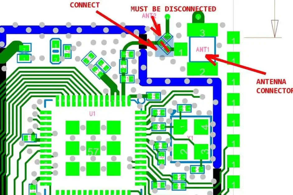
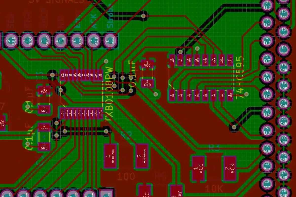
Proper component placement on a PCB or mechanical assembly minimizes assembly errors and improves thermal management. For PCBs, ensure components are spaced at least 7 mil from annular rings and 8 mil from holes to prevent solder mask bridges or misalignment.
-
Actionable Tip: Group components by functionality (e.g., power, signal, or control circuits) to reduce signal interference and simplify soldering. Use automated placement tools to optimize layouts.
-
Example: Placing high-heat components like power transistors away from sensitive ICs can reduce thermal stress, improving reliability by 15%.
5. Simplify Assembly Processes
Complex assembly steps increase labor costs and error rates. Design parts to minimize the number of tools or operations required. For instance, reducing the number of unique fasteners from five to two can decrease assembly time by 20%.
-
Actionable Tip: Use modular designs to break complex assemblies into subassemblies that can be built and tested independently. For PCBs, ensure footprints match datasheet specifications to avoid rework.
-
Example: A modular PCB design with pre-assembled daughterboards can reduce final assembly time by 30% compared to a single, complex board.
6. Incorporate Poka-Yoke (Mistake-Proofing)
Poka-yoke techniques prevent assembly errors by designing parts that can only be assembled correctly. For example, asymmetrical features or unique connectors ensure components are installed in the right orientation.
-
Actionable Tip: Use polarized connectors or keyed slots in PCB designs to eliminate orientation errors. Verify polarity markings are clear in assembly drawings.
-
Example: A keyed USB-C connector prevents incorrect insertion, reducing assembly errors by 10% compared to non-polarized connectors.
7. Ensure Proper Tolerances
Overly tight tolerances increase manufacturing costs without always improving performance. For PCBs, avoid specifying tolerances below 5 mil unless necessary, as tighter tolerances can increase fabrication costs by 15-20%.
-
Actionable Tip: Review process capabilities of your manufacturing equipment and specify tolerances within those limits. For mechanical parts, use chamfers or fillets to accommodate slight misalignments.
-
Example: Specifying a 7 mil clearance for component-to-hole spacing on a PCB ensures compatibility with standard SMT processes, avoiding costly rework.
8. Verify Footprint and BOM Accuracy
Mismatched footprints or incorrect Bill of Materials (BOM) entries can halt production. For instance, a footprint for an 0806 resistor when the BOM specifies an 0402 can lead to assembly delays and additional costs.
-
Actionable Tip: Cross-check all footprints against component datasheets and verify BOM details, including manufacturer part numbers (MPNs) and quantities.
-
Example: Using automated DFA software to validate footprints can reduce errors by 25%, ensuring a smooth transition from design to assembly.
9. Facilitate Testing and Inspection
Designs should include features that simplify testing and inspection, such as test points or accessible solder joints. This reduces quality control time and improves yield rates.
-
Actionable Tip: Add test points for critical nets on PCBs and ensure solder joints are visible for automated optical inspection (AOI). Maintain a 1.6 mil solder mask clearance to prevent short circuits.
-
Example: Including test points for power and ground nets can reduce testing time by 10 minutes per board, improving production throughput.
Integrating DFA into Your Workflow
To effectively implement DFA, follow these steps:
-
Baseline Analysis: Document the current assembly process, including time studies and defect rates, to establish a benchmark.
-
Cross-Functional Teams: Involve design, manufacturing, and quality engineers to identify assembly challenges early.
-
Product Teardown: Disassemble prototypes to pinpoint time-consuming or error-prone steps.
-
Apply DFA Metrics: Use tools like Boothroyd Dewhurst DFA software to quantify assembly efficiency and suggest improvements.
-
Iterate and Validate: Redesign based on DFA findings and validate through prototypes to confirm cost and time savings.
By embedding DFA principles into your design process, you can achieve significant cost reductions and improve product reliability. For example, a case study from the automotive industry showed that applying DFA reduced assembly time by 40% and cut production costs by 30% for a dashboard module.
How ALLPCB Supports DFA Implementation
At ALLPCB, we understand the importance of DFA in achieving cost-effective and reliable designs. Our quick-turn prototyping services allow engineers to test and refine DFA-optimized designs rapidly, ensuring issues are caught early. With global logistics and advanced manufacturing capabilities, we provide high-quality PCB assembly that aligns with DFA principles, such as precise component placement and standardized processes. Our team of experts also offers DFA reviews as part of our turnkey PCB assembly service, helping you identify opportunities to simplify designs and reduce costs without compromising quality.

Conclusion
Implementing DFA principles is essential for engineers aiming to design products that are cost-effective, reliable, and easy to assemble. By following this checklist—minimizing part counts, standardizing components, incorporating self-locating features, and more—you can streamline the assembly process and reduce production costs. Integrating DFA early in the design phase not only saves time and money but also enhances product quality, giving you a competitive edge in the market. Start applying these DFA guidelines today to transform your designs and achieve manufacturing excellence.


