ALLPCB


If you're diving into the world of PCB design and assembly, understanding component placement rules for Surface Mount Technology (SMT) is crucial. Proper SMT component placement ensures your board functions correctly, avoids manufacturing issues, and maintains signal integrity. In this comprehensive guide, we'll cover the essential guidelines for surface mount design, tips for PCB assembly SMT, and best practices for automated placement to help you create efficient and reliable designs.
What is Surface Mount Technology (SMT) and Why Does Placement Matter?
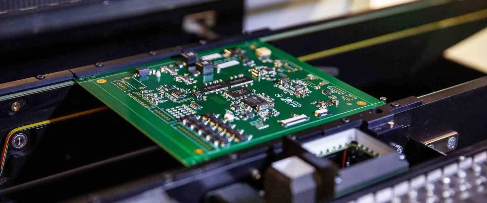
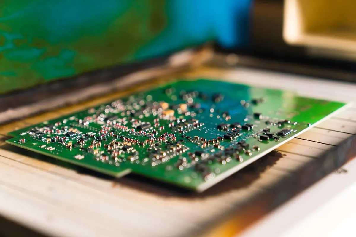
Surface Mount Technology (SMT) is a method used to mount electronic components directly onto the surface of a printed circuit board (PCB). Unlike through-hole technology, which requires drilling holes for component leads, SMT allows for smaller components and denser layouts, making it ideal for modern, compact electronics. However, with this compactness comes the challenge of precise placement. Poor SMT component placement can lead to issues like signal interference, overheating, or assembly errors during automated placement processes.
Effective placement rules ensure that components are positioned for optimal performance, manufacturability, and reliability. Whether you're a beginner or an experienced engineer, following SMT guidelines can save time, reduce costs, and improve the quality of your PCB assembly SMT projects.
Key Principles of SMT Component Placement
Before diving into specific rules, let’s explore the core principles that guide SMT component placement. These principles focus on functionality, manufacturability, and ease of assembly, especially when using automated placement machines.
- Signal Integrity: Components must be placed to minimize noise and interference, especially for high-speed signals.
- Thermal Management: Heat-generating components should be spaced to prevent overheating and ensure proper heat dissipation.
- Manufacturability: Placement must accommodate the capabilities of automated pick-and-place machines and soldering processes.
- Accessibility: Components should be positioned for easy inspection, testing, and rework if needed.
With these principles in mind, let’s break down the specific SMT guidelines for effective surface mount design.
Essential SMT Component Placement Rules
1. Maintain Proper Spacing Between Components
Spacing is one of the most critical factors in SMT component placement. Components placed too close together can cause soldering defects like bridging, where solder connects adjacent pads unintentionally. On the other hand, excessive spacing wastes valuable board space.
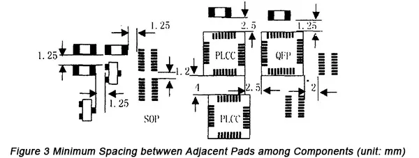
As a general rule, maintain a minimum clearance of 0.2 mm (8 mils) between components for standard designs. For high-density layouts, consult your assembly house for specific tolerances, as automated placement machines may require tighter or looser spacing based on their precision. For example, components like 0201 resistors (0.6 mm x 0.3 mm) often need at least 0.1 mm clearance to avoid issues during reflow soldering.
2. Orient Components for Automated Placement
Automated placement machines, or pick-and-place machines, are widely used in PCB assembly SMT to position components quickly and accurately. To support this process, orient components in a consistent direction whenever possible. For instance, align diodes, capacitors, and resistors in the same direction to minimize machine head rotation during assembly, which speeds up production and reduces errors.
Additionally, ensure that component markings (like polarity indicators on capacitors) are visible and consistent across the board. This helps during inspection and prevents misplacement of polarized components, which could lead to circuit failure.
3. Place High-Speed Components Strategically
For designs involving high-speed signals, such as those operating above 100 MHz, component placement directly impacts signal integrity. Place sensitive components, like microcontrollers or RF modules, close to their associated circuitry to minimize trace lengths. Long traces can introduce parasitic capacitance and inductance, leading to signal degradation. For instance, a trace length of just 10 mm can add a delay of approximately 50 picoseconds, which is significant in high-speed applications.
Also, avoid placing high-speed components near noisy elements like power supplies or switching regulators unless proper shielding or grounding is in place. Use ground planes to reduce electromagnetic interference (EMI) and maintain a clean signal path.
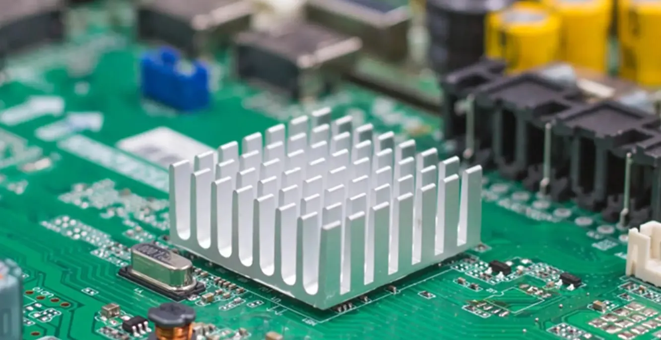
4. Manage Thermal Considerations
Heat dissipation is a major concern in SMT designs, especially for power components like voltage regulators or MOSFETs. Place heat-generating components away from temperature-sensitive parts, such as precision analog ICs, to prevent performance issues. If possible, position these components near the edge of the board or in areas with good airflow for better cooling.
For example, a power IC dissipating 2 watts of heat may require a minimum clearance of 5 mm from neighboring components to avoid thermal coupling. Adding thermal vias or heat sinks near these components can further improve heat management.
5. Group Related Components Together
Grouping related components, such as those in the same functional block (e.g., power supply circuitry), simplifies routing and reduces trace lengths. This not only improves signal integrity but also makes the design easier to debug or modify. For instance, place decoupling capacitors within 1-2 mm of the power pins of an IC to effectively filter noise. A 0.1 μF capacitor placed too far away may fail to stabilize voltage fluctuations during high-frequency operation.
Similarly, keep connectors and interface components near the board’s edge for easy access, while grouping internal logic components centrally to optimize space.
6. Account for Fiducial Marks and Tooling Holes
Fiducial marks are small reference points on the PCB used by automated placement machines to align components accurately. Place at least two fiducial marks on diagonally opposite corners of the board, with a minimum diameter of 1 mm and a clearance of 5 mm from other features. These marks ensure precise component placement during PCB assembly SMT.
Tooling holes, typically unplated and with a diameter of around 3.2 mm (0.127 inches), are also essential for securing the board during assembly. Keep components and traces at least 3 mm away from these holes to avoid interference.
Advanced SMT Guidelines for Complex Designs
1. Consider Panelization for Mass Production
For large-scale production, PCBs are often assembled in panels containing multiple boards. During SMT component placement, ensure that components near panel edges have extra clearance (at least 5 mm) to account for depanelization processes like routing or scoring. This prevents damage to components during separation.
Additionally, avoid placing tall components near panel edges, as they may interfere with assembly equipment or cause uneven stress during handling.
2. Optimize for Reflow Soldering
Reflow soldering is the most common method for attaching SMT components to PCBs. To ensure successful soldering, balance the thermal mass across the board by distributing large and small components evenly. Uneven thermal mass can lead to inconsistent heating, causing defects like tombstoning, where one end of a component lifts off the pad.
For instance, avoid clustering large components like transformers on one side of the board while placing tiny 0402 resistors on the other. This imbalance can result in temperature differences of up to 20°C during reflow, increasing the risk of soldering issues.
3. Plan for Double-Sided Assembly
In double-sided SMT designs, components are placed on both sides of the PCB to maximize space. However, this introduces challenges during assembly. Place heavier components on the bottom side to prevent them from falling off during the second reflow cycle. Also, ensure that components on opposite sides do not overlap in a way that causes mechanical stress or heat buildup.
For example, avoid placing a large IC directly above a power resistor on the opposite side, as the combined heat could exceed safe operating temperatures (typically around 85°C for many components).
Common Mistakes to Avoid in SMT Component Placement
Even with the best intentions, mistakes in surface mount design can lead to costly rework or failed boards. Here are some pitfalls to watch out for:
- Ignoring Design for Manufacturability (DFM): Failing to consult assembly guidelines can result in layouts that are difficult or impossible to manufacture. Always check with your assembly partner for specific constraints.
- Overcrowding Components: Packing components too tightly may save space but often leads to soldering defects or assembly errors.
- Neglecting Polarity Markings: Incorrect orientation of polarized components like diodes or electrolytic capacitors can cause circuit failure.
- Poor Trace Routing After Placement: Component placement should be planned alongside routing to avoid long, noisy traces or unnecessary vias.
Tools and Resources for SMT Component Placement
Modern PCB design software offers features to assist with SMT component placement. Tools like auto-placement algorithms can suggest optimal layouts based on design rules, while design rule checks (DRC) help identify spacing violations or other issues before manufacturing. Additionally, many assembly houses provide DFM guidelines tailored to their equipment, which can be invaluable for ensuring a smooth PCB assembly SMT process.
Staying updated with industry standards, such as those from the Institute of Printed Circuits (IPC), can also guide your designs. For example, the IPC-7351 standard provides detailed recommendations for land patterns and component spacing in SMT designs.
Conclusion: Mastering SMT Component Placement for Better Designs
Effective SMT component placement is a blend of art and science, requiring attention to detail and an understanding of both design and manufacturing constraints. By following the SMT guidelines outlined in this post—such as maintaining proper spacing, orienting components for automated placement, and managing thermal considerations—you can create reliable, high-performing PCB layouts. Whether you're working on a simple prototype or a complex, high-density board, these rules for surface mount design will help streamline your PCB assembly SMT process and ensure success.
Take the time to plan your layouts carefully, leverage design tools, and collaborate with your assembly partner to address any specific requirements. With these practices in place, you’ll be well on your way to mastering SMT component placement and delivering top-quality electronic designs.