ALLPCB


Ball Grid Array (BGA) assembly is a cornerstone of modern electronics manufacturing, enabling the creation of compact, high-performance devices like smartphones, laptops, and medical equipment. The BGA package's ability to pack numerous connections into a small footprint has made it indispensable, but its soldering process is complex due to hidden solder joints beneath the component. For engineers, mastering reliable BGA soldering techniques is critical to ensure durability and functionality. In this blog, we'll explore the essential steps, challenges, and best practices for BGA assembly, offering actionable insights to help you achieve top-quality results.
Whether you're designing a cutting-edge microprocessor or troubleshooting a prototype, understanding BGA soldering can make or break your project. Let's dive into the techniques that ensure strong, reliable solder joints every time.
Understanding BGA Packages
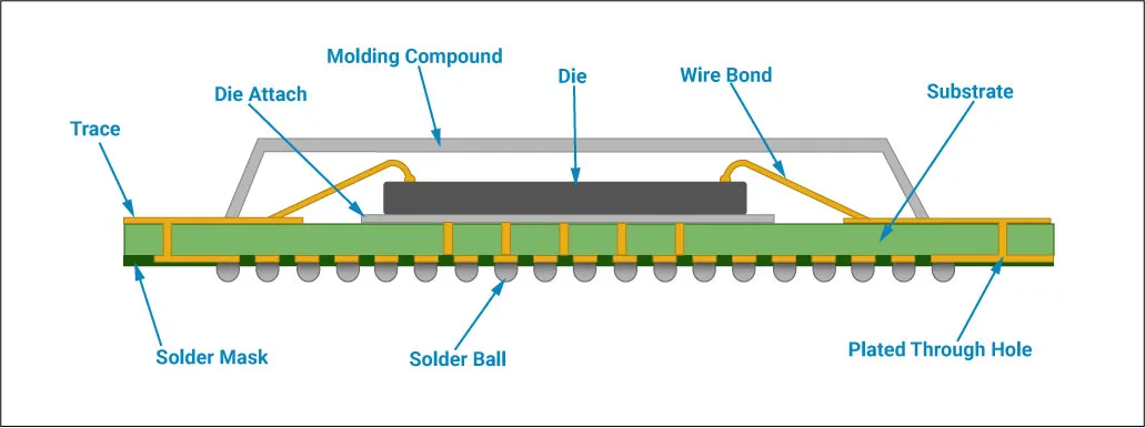
A Ball Grid Array (BGA) is a surface-mount package where solder balls on the underside connect an integrated circuit (IC) to a printed circuit board (PCB). Unlike traditional leaded packages, BGAs use these balls to create high-density connections, making them ideal for applications requiring significant pin counts in a small space. Their compact design and excellent electrical performance have made them a go-to choice for everything from consumer electronics to aerospace systems.
BGA packages vary to suit different needs:
- Plastic BGA (PBGA): Affordable and widely used in devices like gaming consoles, PBGAs feature a plastic substrate.
- Ceramic BGA (CBGA): With superior thermal conductivity, CBGAs shine in high-performance settings like servers or automotive electronics.
- Tape BGA (TBGA): Lightweight and flexible, TBGAs are common in slim devices such as wearables.
The pitch - the distance between solder balls - can range from 1.27mm in older designs to as tight as 0.4mm in advanced packages, demanding precision in every assembly step.
Key Techniques for Reliable BGA Soldering
Soldering BGAs successfully requires a systematic approach, from PCB design to final inspection. Below are the critical techniques to master.
1. PCB Design and Layout Considerations
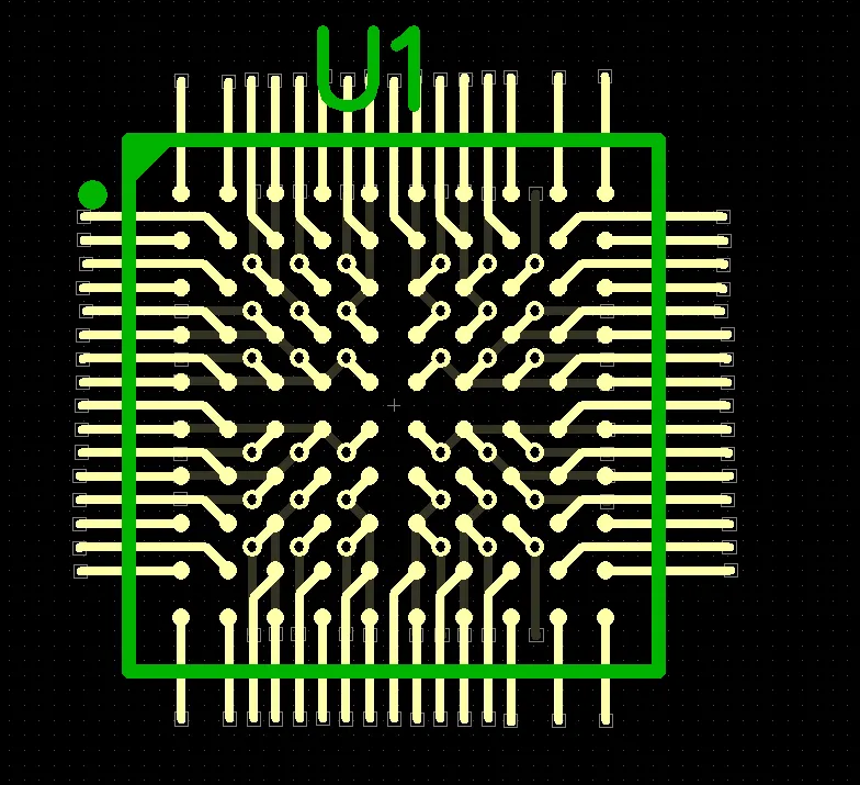
A well-designed PCB sets the stage for reliable BGA soldering. The layout must align perfectly with the BGA's specifications to prevent issues like misalignment or weak joints.
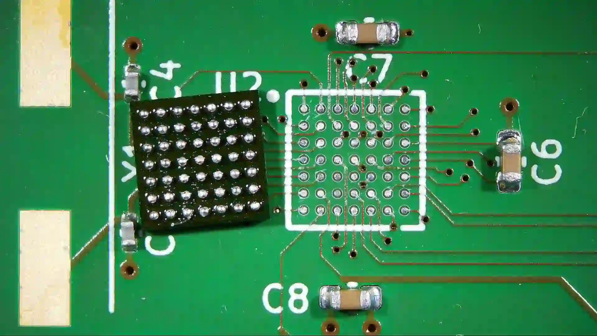
- Footprint Accuracy: The PCB's pad pattern must match the BGA's ball layout. For a 0.8mm pitch BGA, pads might be 0.4mm in diameter, while a 0.4mm pitch requires smaller, precisely spaced pads.
- Via Management: Avoid unfilled vias under pads, as they can wick solder away, causing voids. Use plugged or capped vias if necessary.
- Solder Mask Choice: Non-solder mask defined (NSMD) pads improve joint strength for pitches of 0.5mm or larger by allowing solder to wrap around the pad edges.
2. Solder Paste Application
Solder paste bridges the BGA balls to the PCB pads, so its application must be flawless. Most assemblies today use lead-free solder (e.g., SAC305 alloy) for compliance with RoHS standards.
- Stencil Thickness: A 100-150μm thick laser-cut stencil suits most BGAs. For a 0.5mm pitch, 125μm is typical to balance paste volume.
- Aperture Design: Circular apertures ensure even paste deposition. A 1:1 aperture-to-pad ratio works for larger pitches, while a slight reduction (e.g., 90%) helps finer pitches avoid excess paste.
- Paste Control: Too much paste risks bridges; too little starves the joint. Aim for a consistent 0.1-0.15mm³ per pad.
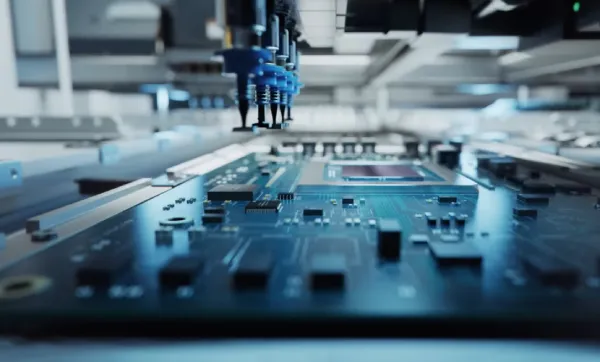
3. Component Placement
Placing the BGA accurately ensures every ball contacts its pad. Precision here prevents costly rework.
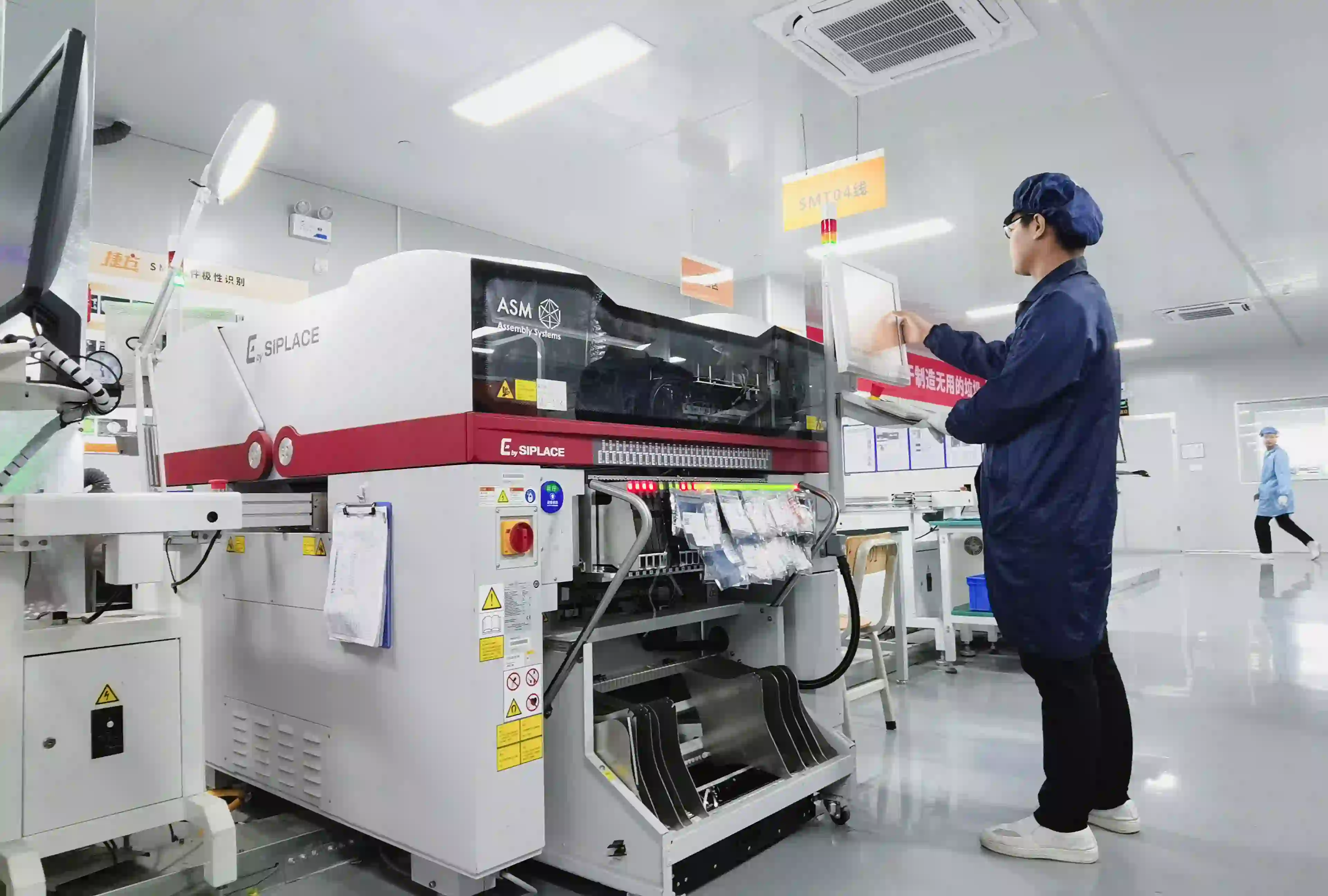
- Equipment: High-end pick-and-place machines with vision systems can achieve ±25μm accuracy, vital for pitches below 0.5mm.
- Alignment Aids: Fiducial marks - small reference points on the PCB - guide the machine to position the BGA perfectly.
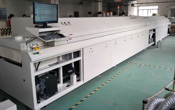
4. Reflow Soldering
Reflow soldering melts the paste to form solid joints. The temperature profile must be tailored to the solder type and PCB assembly.
- Profile Basics: For lead-free solder, preheat to 150-180°C, soak for 60-90 seconds, then peak at 235-250°C for 20-40 seconds.
- Even Heating: A controlled soak minimizes thermal gradients, ensuring all balls melt uniformly under the BGA.
- Cooling: Cool at 2-4°C per second to avoid cracks or stress in the joints.
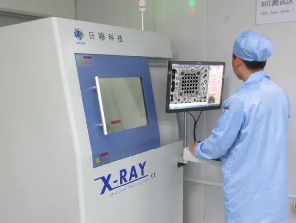
5. Inspection and Quality Control
Since BGA joints are hidden, standard visual checks won't cut it. Advanced methods are essential.
- X-Ray Inspection: Automated X-ray systems reveal voids (bubbles in the solder), bridges, or missing joints. A void rate below 25% is generally acceptable per IPC standards.
- Functional Testing: Electrical tests confirm connectivity but can miss structural flaws, so pair them with X-ray for thoroughness.
Common Challenges in BGA Soldering and Solutions
Even with careful planning, BGA soldering can encounter hurdles. Here's how to tackle the most frequent issues.
1. Solder Joint Voids
Voids reduce joint strength and conductivity. They often form when flux gases get trapped during reflow.
- Solution: Extend the soak phase to 90-120 seconds, letting gases escape before the solder hardens.
2. Solder Bridging
Excess solder can connect adjacent balls, shorting the circuit.
- Solution: Refine stencil apertures and reduce paste volume slightly. Check alignment to avoid smearing during placement.
3. Misalignment
A misaligned BGA can leave open circuits or weak joints.
- Solution: Verify machine calibration and fiducial mark clarity. Post-placement inspection with a camera can catch errors early.
4. Thermal Stress
BGAs in high-power applications generate heat, risking joint failure over time.
- Solution: Add thermal vias (e.g., 0.3mm diameter, 1mm spacing) under the BGA or attach a heat sink.
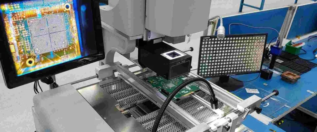
Rework and Repair Techniques
When defects slip through, rework becomes necessary. BGA rework demands precision to protect the PCB and component.
- Tools: A BGA rework station with top and bottom heaters maintains controlled temperatures (e.g., 220-240°C for removal).
- Process: Heat the BGA, lift it with a vacuum tool, clean the site with a solder wick, then apply fresh paste for a new component.
- Caution: Limit rework cycles - typically two - to avoid PCB damage.
Why Precision Matters in BGA Assembly
Reliable BGA soldering isn't just about avoiding defects; it's about ensuring long-term performance. A single weak joint can fail under thermal cycling or vibration, common in automotive or aerospace applications. By nailing each step - design, paste, placement, reflow, and inspection - you minimize risks and maximize product lifespan.
For engineers tackling complex projects, partnering with an expert manufacturer can streamline the process. At ALLPCB, we offer quick-turn prototyping and advanced manufacturing tailored to BGA assembly needs. Our global logistics ensure your boards arrive fast, while our precision equipment handles pitches down to 0.4mm with ease. Whether you're iterating a design or scaling production, we've got your back.
Conclusion
BGA assembly combines challenge and opportunity. With the right techniques - thoughtful PCB design, precise solder paste application, accurate placement, optimized reflow, and rigorous inspection - you can achieve solder joints that stand the test of time. Overcoming pitfalls like voids or bridging takes diligence, but the payoff is a robust, high-performing device.
Ready to elevate your BGA projects? Explore how ALLPCB's expertise can support your next build, delivering quality and speed to bring your ideas to life.