 ALLPCB


Metal-backed PCBs, also known as metal core or insulated metal substrate boards, play a vital role in applications that demand efficient heat dissipation. Engineers often encounter specific design challenges when working with these boards, including thermal expansion mismatches, mechanical stress, and electrical isolation concerns. Addressing metal-backed PCB design issues early in the layout phase helps maintain reliability and performance across demanding operating conditions. This article examines frequent problems, their underlying mechanisms, and practical approaches to resolution.
Understanding Metal-Backed PCB Designs and Their Importance
Metal-backed PCBs consist of a dielectric layer bonded to a metal substrate, typically aluminum or copper, which serves as both a heat spreader and mechanical support. These constructions excel in high-power environments where conventional FR-4 boards would overheat rapidly. Proper thermal management remains essential because the metal core conducts heat away from components far more effectively than standard laminates. Engineers must balance electrical performance with mechanical stability when selecting stack-up configurations. Industry relevance continues to grow in sectors such as automotive lighting, power converters, and LED arrays.
Common PCB Design Problems in Metal-Backed Boards
Designers frequently report warpage during thermal cycling, delamination at the dielectric-metal interface, and uneven copper trace adhesion. Thermal management problems arise when via placement fails to provide adequate heat paths to the metal core. Electrical isolation can degrade if the dielectric thickness varies or contains voids. Mechanical drilling and routing operations sometimes introduce micro-cracks that propagate under vibration. These issues collectively reduce yield and shorten product lifespan when left unaddressed.
Related Reading: Designing for Reliability: Best Practices for Insulated Metal Substrate PCB Layout
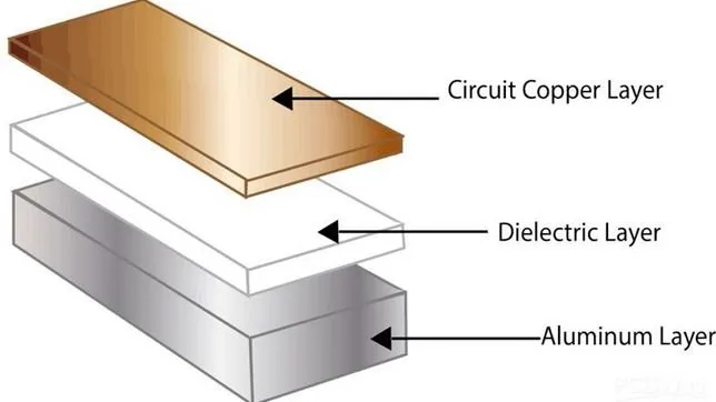
Technical Principles and Mechanisms Causing Failures
Coefficient of thermal expansion differences between the metal substrate and copper layers generate internal stresses during temperature changes. Heat flow follows the path of least thermal resistance, so insufficient thermal vias concentrate temperature gradients near high-power components. Dielectric materials experience viscoelastic relaxation under sustained load, which can weaken adhesion over time. Per IPC-6012E, qualification testing verifies that boards withstand specified thermal shock and humidity conditions without structural failure. Residual stresses from lamination processes further contribute to dimensional instability when the board is later exposed to reflow temperatures.
Practical Solutions and Best Practices for Metal-Backed PCB Troubleshooting
Engineers should begin by modeling thermal performance using finite-element analysis before finalizing the layout. Placing thermal vias in a grid pattern beneath heat-generating components improves heat transfer to the metal core. Selecting dielectric materials with matched expansion coefficients reduces warpage risk. Controlled lamination pressure and temperature profiles during manufacturing help maintain uniform bond strength. Designers also benefit from incorporating strain-relief features such as slotted mounting holes in the final assembly.
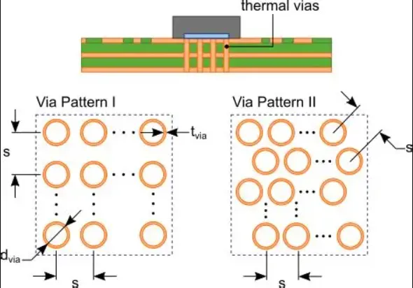
Additional steps include specifying minimum dielectric thickness based on voltage isolation requirements and verifying copper weight consistency across the board. Routing traces away from high-stress zones near board edges minimizes crack initiation. Regular design reviews that incorporate thermal imaging data allow iterative refinement before production release.
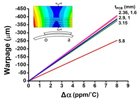
Troubleshooting Insights for Electric Engineers
When boards exhibit unexpected thermal hotspots, engineers first inspect via fill quality and dielectric uniformity through cross-section analysis. Warpage exceeding acceptable limits often traces back to asymmetric copper distribution or improper baking prior to assembly. Electrical leakage problems typically result from moisture ingress at the metal-dielectric boundary, which can be mitigated by applying conformal coatings after thorough drying. Systematic root-cause analysis using fishbone diagrams helps isolate whether the issue originates in design, material selection, or process parameters.
Related Reading: Metal Core PCBs: The Secret Weapon for High Power Thermal Management
Conclusion
Effective resolution of metal-backed PCB design issues requires attention to thermal, mechanical, and electrical interactions from the earliest design stages. Structured application of best practices reduces the incidence of warpage, delamination, and thermal management problems. Engineers who integrate simulation, material compatibility checks, and process controls achieve higher reliability in finished products. Continued adherence to established qualification methods supports consistent performance across production lots.
FAQs
Q1: What are the most frequent metal-backed PCB design issues engineers face?
A1: Common problems include warpage, poor thermal dissipation, and dielectric delamination. These arise primarily from thermal expansion mismatches and inadequate via placement. Addressing them during layout prevents costly rework later in the product cycle.
Q2: How can thermal management problems be resolved in metal-backed PCB troubleshooting?
A2: Engineers improve heat flow by adding dense thermal via arrays and selecting high-conductivity dielectrics. Proper stack-up design and finite-element thermal modeling further reduce temperature gradients. These steps ensure components remain within safe operating limits.
Q3: What standards guide qualification of metal-backed PCBs?
A3: IPC-6012E outlines performance requirements for rigid printed boards, including thermal and mechanical testing protocols. JEDEC J-STD-020E addresses moisture sensitivity considerations during reflow. Compliance with these documents helps verify long-term reliability.
Q4: Why does PCB design solutions emphasis on material selection matter?
A4: Choosing dielectrics with expansion coefficients close to the metal core minimizes internal stresses. Consistent copper thickness and controlled lamination parameters further enhance mechanical stability. Such choices directly influence both yield and field performance.
References
IPC-6012E — Qualification and Performance Specification for Rigid Printed Boards. IPC, 2017
JEDEC J-STD-020E — Moisture/Reflow Sensitivity Classification. JEDEC, 2014





