 ALLPCB


Introduction
Copper has long served as the cornerstone conductor material in printed circuit boards due to its superior electrical conductivity and cost-effectiveness. As electronics evolve toward higher frequencies, denser interconnects, and greater power demands, the future of copper in electronics faces both opportunities and challenges. Innovations in copper processing and emerging PCB copper alternatives promise to address limitations like signal loss at high speeds and thermal constraints in compact designs. Engineers must stay informed on advanced copper materials PCB to optimize performance in applications from 5G infrastructure to electric vehicles. This article explores key trends shaping copper's role, drawing on established engineering principles and industry standards.
The Enduring Role of Copper in PCB Design
Copper's dominance stems from its low resistivity, which enables efficient current flow and minimal voltage drop across traces. In multilayer boards, copper layers form the backbone for signal routing, power distribution, and ground planes, ensuring reliable operation under varying loads. Despite advances in other metals, copper balances manufacturability with performance, adhering to specifications like IPC-6012 for rigid board qualification. Its ductility allows for fine-line etching down to microns, critical for high-density interconnects. However, as operating frequencies push into millimeter-wave ranges for 6G, skin effect increases resistance, prompting refinements in copper surface treatment. Engineers appreciate copper's compatibility with standard plating processes, which enhance via reliability and solder joint integrity.
Challenges arise from electromigration in high-current paths, where atomic diffusion under electric fields degrades traces over time. Thermal expansion mismatches between copper and dielectrics can induce stress during reflow soldering, as outlined in IPC-A-600 acceptability criteria. Yet, copper's thermal conductivity aids heat spreading, vital for power electronics. These properties position copper as irreplaceable for now, but ongoing research targets enhancements for the future of copper in electronics.
Advancements in Copper Foil Technology
Modern PCB fabrication relies on specialized copper foils to meet signal integrity demands. Electrodeposited (ED) foils offer strong adhesion to laminates, ideal for rigid boards with high layer counts. Rolled-annealed (RA) foils provide superior flexibility and fatigue resistance, suiting dynamic flex circuits. Recent innovations include low-profile (LP) and very low-profile (VLP) foils, which minimize surface roughness to reduce insertion loss at high frequencies. These advanced copper materials PCB feature smoother dendrites, improving impedance control and reducing attenuation in 5G base stations. Hyper very low-profile (HVLP) variants further optimize for terahertz signals in emerging 6G prototypes.
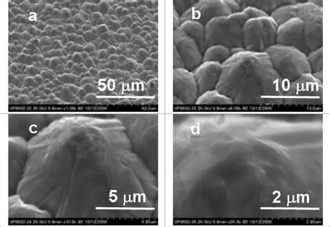
Reverse-treated foils (RTF) enhance peel strength while maintaining flatness, preventing warpage in sequential build-up processes. Horizontal traffic electrodeposited (HTE) foils deliver uniform thickness and thermal stability, minimizing cracks during lamination cycles. These developments align with J-STD-001 requirements for soldered assemblies, ensuring robustness in harsh environments. Engineers selecting foils must consider foil weight, from 1 oz for fine-pitch signals to 10 oz for power planes. Such tailored foils extend copper's viability into next-generation designs.
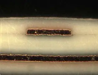
Heavy Copper Solutions for Power and Thermal Management
Heavy copper PCBs, with outer layers exceeding 3 oz/ft2, excel in high-current applications like inverters and motor drives. Thicker copper reduces I2R losses, allowing compact layouts without excessive heating. Copper-inlaid or coin-embedded structures embed pure copper blocks into cores for localized heat sinking, outperforming traditional vias. This approach leverages copper's 400 W/mK conductivity to channel heat away from components, critical for LEDs and RF amplifiers. Manufacturing involves progressive etching and differential plating to maintain trace geometry under high aspect ratios.
In power electronics, heavy copper mitigates hotspot formation, extending component life. Compliance with IPC-2221 design guidelines ensures current-carrying capacity matches trace width and temperature rise limits. These boards support automotive electrification trends, where vibration and thermal cycling demand durability. Engineers benefit from finite element analysis to predict stress distributions in heavy copper stacks.
Low-Loss Copper for High-Frequency Applications
At frequencies above 10 GHz, copper surface roughness dominates signal loss via skin effect, where currents concentrate on foil peaks. Advanced copper materials PCB with ultra-low roughness profiles counteract this, preserving return loss in microstrip lines. For 5G and beyond, low-Dk dielectrics pair with treated foils to achieve low insertion loss. Profiled foils like double matte or filled micro-roughened variants balance adhesion and smoothness, adhering to high-speed laminate specs.
Engineers model roughness impact using scattering parameters, selecting foils based on frequency and dielectric constant. These innovations enable denser routing without equalization circuits, simplifying designs. In radar and mmWave modules, such copper maintains phase linearity across bands.
PCB Copper Alternatives: Viable Contenders?
While copper prevails, PCB copper alternatives emerge for niche roles. Aluminum offers lower cost and weight, with resistivity about 60% higher, suiting low-speed power interconnects. Its oxide layer provides natural passivation, but bonding requires specialized anodizing. Graphene-assembled films show promise for flexible high-frequency antennas, exhibiting lower loss than copper at extreme frequencies due to ballistic conduction. Carbon nanotube inks enable printed traces on unconventional substrates, bypassing etching waste.
These alternatives face scalability hurdles, including contact resistance and environmental stability. Silver nanowires provide high conductivity but oxidize readily. Engineers evaluate alternatives via figure-of-merit metrics like conductivity-to-weight ratio. For now, hybrids like copper-graphene composites bridge gaps, enhancing electromigration resistance.
Sustainability Trends in Copper Usage
Recycling copper from end-of-life PCBs recovers over 90% of metal content via smelting, reducing mining demands. Advanced hydrometallurgical processes yield nano-copper powders for foil production, minimizing energy use. Low-waste etching solutions and closed-loop plating reclaim copper ions, aligning with ISO 14001 environmental standards. Engineers prioritize designs facilitating delamination, such as modular stacks.
Biodegradable substrates paired with thin copper layers cut e-waste volume. These practices support circular economy models without compromising IPC class 3 performance.
Best Practices for Implementing Advanced Copper Innovations
Select copper foils based on application: LP for signals, heavy for power. Simulate thermal profiles early to validate layer sequencing. Use orthogonal weave laminates with low-profile copper to curb skew in differential pairs. Validate via IPC coupon testing for peel strength and impedance. Prototype with sequential lamination for complex builds.
Collaborate on DFM reviews to optimize drill sizes for heavy copper. Monitor foil uniformity via cross-section analysis post-fabrication.
Conclusion
The future of copper in electronics thrives on refined foils, heavy constructions, and selective alternatives, addressing density, speed, and efficiency needs. Advanced copper materials PCB evolve to support 5G/6G and electrification without full replacement. Engineers leveraging these trends ensure reliable, future-proof designs. Standards like IPC-6012 guide adoption, fostering innovation grounded in proven practices.
FAQs
Q1: What are the main advanced copper materials PCB for high-frequency designs?
A1: Low-profile and very low-profile foils reduce surface roughness, minimizing skin effect losses in 5G applications. These materials maintain adhesion while enabling finer lines and better impedance control. Select based on frequency and laminate pairing for optimal signal integrity.
Q2: How do PCB copper alternatives compare to traditional copper?
A2: Alternatives like aluminum offer cost savings for power but higher resistivity limits signal use. Emerging graphene films excel at mmWave due to low loss, though scalability lags. Copper remains preferred for balanced performance in most electronics.
Q3: What drives the future of copper in electronics?
A3: Demand from EVs, renewables, and 6G pushes heavy copper and low-roughness foils. Sustainability via recycling enhances viability. Innovations ensure copper adapts to miniaturization and high power without obsolescence.
Q4: When should engineers consider heavy copper in PCBs?
A4: Use for high-current paths in power supplies where thermal management is critical. It reduces losses and supports compact layouts per IPC-2221 guidelines. Ideal for automotive and industrial boards under thermal stress.
References
IPC-6012E — Qualification and Performance Specification for Rigid Printed Boards. IPC, 2018
IPC-A-600K — Acceptability of Printed Boards. IPC, 2020
IPC-2221 — Generic Standard on Printed Board Design. IPC, 2012
J-STD-001H — Requirements for Soldered Electrical and Electronic Assemblies. IPC, 2018


