 ALLPCB


Introduction
In analog signal PCBs, maintaining clean signal paths is crucial for reliable performance, especially in applications like sensors, amplifiers, and data acquisition systems. Trace width plays a pivotal role in trace width noise reduction by influencing resistance, inductance, and capacitance along the signal path. Improper sizing can amplify noise from crosstalk, electromagnetic interference, or ground bounce, degrading signal integrity. Engineers must balance trace dimensions with layout constraints to preserve waveform fidelity. This article explores how to select optimal trace widths for analog signals, integrates grounding techniques, and outlines best practices aligned with industry standards. By understanding these elements, designers can achieve robust analog signal PCB layouts that withstand real-world noise challenges.
Why Trace Width Matters for Analog Signal PCBs
Analog signals are particularly susceptible to noise due to their continuous nature and sensitivity to environmental disturbances. Narrow traces increase series resistance and inductance, leading to voltage drops and higher susceptibility to inductive coupling from nearby high-speed lines. Conversely, excessively wide traces can elevate parasitic capacitance, which distorts low-frequency responses or introduces coupling between adjacent signals. Proper trace width selection directly impacts signal integrity by controlling characteristic impedance and minimizing attenuation over distance. In multi-layer boards, trace width also affects how effectively signals couple to reference planes, influencing return current paths. For electric engineers, recognizing these trade-offs ensures compliance with performance specifications in precision circuits.
The relevance extends to system-level reliability, where noise accumulation can cascade through amplification stages, resulting in measurable errors. Standards like IPC-2221 provide foundational guidelines for trace dimensions, emphasizing the need for calculations based on current, frequency, and board stackup. Ignoring trace width optimization often leads to iterative redesigns during prototyping.
Technical Principles of Noise in Analog Traces
Noise in analog signal PCBs arises from multiple coupling mechanisms, including capacitive, inductive, and conductive paths. Capacitive coupling occurs when electric fields between parallel traces induce voltage fluctuations, proportional to trace width and proximity. Inductive coupling, dominant at higher frequencies, depends on loop area formed by the trace and its return path; narrower traces reduce this area but heighten resistance. Electromagnetic interference from external sources penetrates via antenna-like trace structures, where longer, thinner traces act as better receivers. Grounding techniques mitigate these by providing low-impedance return paths, shunting noise to ground before it corrupts the signal.
Signal integrity suffers when impedance mismatches cause reflections, exacerbated by inconsistent trace widths along the path. Parasitic effects scale with frequency: for audio-range signals up to 20 kHz, resistance dominates, while RF analog demands controlled impedance. Engineers model these using transmission line theory, where trace width determines Z0 alongside dielectric thickness and spacing.
How Trace Width Influences Trace Width Noise Reduction
Selecting trace width begins with signal characteristics: voltage level, frequency content, and expected current. Wider traces lower DC resistance, reducing thermal noise from Johnson-Nyquist effects, but increase fringing fields that couple to neighbors. A balanced approach uses widths around 0.2 to 0.5 mm for general analog signals, adjusted for layer and stackup. In practice, simulations reveal that doubling width halves inductance but may raise capacitance by 20-50%, depending on ground plane proximity. Maintaining uniform width prevents impedance steps that reflect energy back to the source.
For sensitive analog paths, integrate trace width with routing topology: keep lengths short to limit exposure, and route over solid ground planes for image current return. IPC-2221 recommends considering external factors like temperature rise, though signal traces prioritize electrical over thermal limits. This structured sizing minimizes both intrinsic and extrinsic noise sources.
Grounding Techniques for Enhanced Signal Integrity
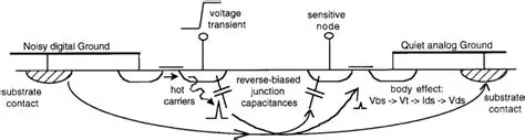
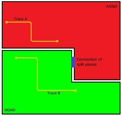
Effective grounding techniques form the backbone of noise suppression in analog signal PCBs. A dedicated analog ground plane, split from digital sections, prevents high-frequency switching noise from injecting into sensitive areas. Connect splits at a single point near the power entry to avoid loops, ensuring star-point topology. Guard traces, grounded at intervals, flank analog lines to absorb stray fields, effectively widening the isolation moat. Stitching vias along plane edges tie layers together, reducing slot antenna effects that radiate or receive EMI.
Return paths must mirror signal traces closely; wider ground pours under traces equalize impedance. In four-layer boards, dedicate inner layers to ground and power, sandwiching signals between for symmetric fields. These methods, combined with trace width optimization, yield signal-to-noise ratios exceeding 80 dB in precision designs.
Best Practices for Analog Signal PCB Design
Start with stackup planning: position analog signals on inner layers adjacent to ground for minimal loop inductance. Route traces perpendicular to potential aggressors, maintaining spacing at least three times the trace width to curb crosstalk. Use differential routing for balanced analog signals, matching trace widths and lengths to reject common-mode noise. Decouple power pins with ceramics near analog components, tying to local ground pours. Verify designs against IPC-A-600 acceptability criteria for trace quality post-fabrication.
Incorporate shielding cans over noisy sections, grounded via multiple vias. For mixed-signal boards, isolate clocks and ADCs with moats wider than trace dimensions. Prototype testing with spectrum analyzers confirms noise floors below -100 dBm/Hz.
Troubleshooting Common Noise Issues
Engineers often encounter hum at 50/60 Hz from poor grounding, resolved by single-point analog-digital ties and ferrite beads on power lines. Crosstalk spikes during sweeps indicate inadequate spacing; widen gaps or add grounded fences. High-frequency jitter points to impedance discontinuities, fixed by tapering widths at vias. Scope probing reveals ground bounce if returns share digital paths; implement separate planes immediately.
Oscilloscope FFTs quantify noise contributions, guiding iterations. Common pitfalls include via stubs acting as resonators, mitigated by back-drilling or blind vias per J-STD-001 assembly standards.
Conclusion
Optimizing trace width for analog signals demands a holistic view of resistance, parasitics, and layout interactions to achieve trace width noise reduction. Grounding techniques like split planes and guards, paired with precise routing, safeguard signal integrity across frequencies. Adhering to IPC guidelines ensures manufacturability and performance. Electric engineers benefit from these practices in delivering noise-resilient designs. Implement simulations early, prototype rigorously, and refine based on measurements for superior outcomes.
FAQs
Q1: What trace width is ideal for low-noise analog signal PCBs?
A1: For analog signal PCBs, widths of 0.2 to 0.5 mm suit most low-frequency applications, balancing resistance and capacitance. Narrower traces reduce coupling but raise inductance; wider ones lower impedance mismatches. Always simulate with stackup details for signal integrity. Ground planes beneath enhance effectiveness.
Q2: How do grounding techniques improve trace width noise reduction?
A2: Grounding techniques like dedicated planes and stitching vias provide low-impedance returns, shunting noise away from analog traces. Split grounds isolate digital switching currents, preventing injection. Guard traces between signals absorb fields, complementing optimal trace widths for cleaner paths.
Q3: Why is signal integrity critical in analog signal PCB design?
A3: Signal integrity preserves waveform shape against noise, reflections, and attenuation in analog signal PCBs. Trace width directly controls impedance and parasitics, vital for precision like instrumentation amps. Poor integrity amplifies errors downstream, demanding structured layouts and standards compliance.
Q4: What role does IPC-2221 play in analog trace design?
A4: IPC-2221 offers guidelines for trace dimensions based on electrical and mechanical needs, aiding trace width noise reduction. It informs sizing for current and voltage, adaptable to analog frequencies. Designers use it alongside simulations for robust signal integrity.
References
IPC-2221B - Generic Standard on Printed Board Design. IPC, 2003
IPC-A-600K - Acceptability of Printed Boards. IPC, 2020
J-STD-001H - Requirements for Soldered Electrical and Electronic Assemblies. IPC, 2020


