 ALLPCB


Introduction
Copper weight represents a fundamental parameter in printed circuit board design, measured in ounces per square foot, where 1oz corresponds to approximately 35 microns of thickness. Electrical engineers often encounter "1oz" as the default specification in PCB stackups, prompting questions like why 1 oz is standard. This choice stems from decades of industry evolution, balancing electrical conductivity, mechanical reliability, and fabrication feasibility. Understanding oz in copper design helps optimize signal integrity, power delivery, and overall board performance. For most applications, from consumer electronics to industrial controls, 1oz delivers sufficient current handling without excessive cost or complexity. This article explores the engineering rationale behind pcb standard thickness choices, particularly the prevalence of 1oz copper.
What Is Copper Weight in PCBs and Why It Matters
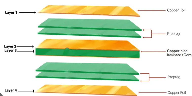
Copper weight defines the mass of copper foil per unit area on a PCB layer, expressed as ounces per square foot, directly translating to thickness since copper density is constant. A 1oz layer means one ounce of copper spread evenly over one square foot, yielding a nominal thickness of 1.37 mils or 35 micrometers before processing. Electrical engineers prioritize this metric because it influences trace resistance, current-carrying capacity, and thermal dissipation. Thicker copper reduces resistance for power traces, while thinner foils enable finer features for high-speed signals. In multilayer boards, outer layers typically start at 1oz for plating compatibility, while inner layers maintain similar weights for lamination integrity. Deviating from pcb standard thickness can impact impedance control and manufacturing yields, making informed selection critical for reliable designs.
Historical Evolution and Manufacturing Foundations of 1oz Standard
The 1oz copper weight emerged as standard during the early days of PCB fabrication when electrodeposited foil processes standardized around this thickness for optimal adhesion and etchability. Fabricators found that 35-micron foil provided a robust base for panel plating, where additional copper builds vias and traces during through-hole processing. Etching 1oz material minimizes undercutting compared to heavier foils, preserving trace geometry and reducing scrap rates. This thickness also aligns with press cycles in multilayer lamination, preventing foil wrinkles or delamination under heat and pressure. Over time, supply chains optimized around 1oz base laminates, making it the economical default for why 1 oz is standard. Electrical engineers benefit from this legacy, as it supports consistent design rules across prototypes and production.
Technical Principles Behind 1oz in Electrical Performance
From an electrical perspective, 1oz copper offers low DC resistance suitable for most signal and moderate power traces, typically handling 1 to 3 amps per mil of width under standard temperature rises. Skin effect at high frequencies confines current to the surface, but 35 microns provides adequate depth for frequencies up to several GHz without significant loss increase. Impedance calculations for microstrips and striplines assume 1oz finished thickness, simplifying stackup modeling in design tools. Thicker copper increases inductance slightly, which can detune controlled-impedance lines unless dielectric heights adjust accordingly. For power integrity, 1oz planes distribute voltage evenly with minimal droop in typical digital circuits. These properties explain oz in copper design as a versatile baseline for electrical engineers tackling mixed-signal boards.
Current-Carrying Capacity and Thermal Considerations
Current capacity scales with copper cross-section, where 1oz traces excel in low-to-medium power scenarios by dissipating heat effectively through convection and conduction. Engineers use empirical charts to size traces, noting that 1oz supports higher densities than heavier weights without excessive width demands. Thermal resistance drops with thickness, but 1oz strikes a balance, avoiding hotspots common in thin foils under sustained loads. In high-reliability designs, plating adds 10-20 microns to outer layers, enhancing via reliability without altering inner layer standards. Board warpage risks increase with asymmetric heavy copper, reinforcing 1oz as pcb standard thickness for flatness. Practical simulations confirm that 1oz maintains junction temperatures within limits for most ICs.
- Copper Weight: 0.5 oz — Nominal Thickness: 18 μm — Typical Max Current per 10 mil Trace (A, 10°C rise): 1.5
- Copper Weight: 1 oz — Nominal Thickness: 35 μm — Typical Max Current per 10 mil Trace (A, 10°C rise): 3
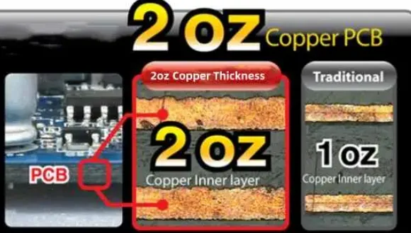
- Copper Weight: 2 oz — Nominal Thickness: 70 μm — Typical Max Current per 10 mil Trace (A, 10°C rise): 6
Signal Integrity and High-Speed Design with 1oz Copper
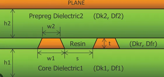
In high-speed designs, 1oz copper facilitates precise impedance control, as trace height post-etch closely matches simulations. Dielectric interactions dominate losses at RF, where 35-micron thickness minimizes conductor attenuation without excessive surface roughness. Engineers specify 1oz for outer layers to support fine-pitch routing, essential for DDR or PCIe interfaces. Return path integrity benefits from plane proximity, with 1oz providing sufficient shielding. Fabrication tolerances per industry norms ensure repeatability, critical for eye diagram margins. Thus, why 1 oz is standard persists in demanding electrical environments.
Practical Best Practices for Specifying Copper Weight
Start with 1oz for all layers unless power demands exceed 5 amps per trace, then consider 2oz on dedicated planes. Verify stackup symmetry to prevent bow and twist, using 1oz inners for balance. Communicate "start copper" versus "finished copper" clearly, accounting for 10-15% etch loss. For HDI boards, drop to 0.5oz on select layers for microvia fanout. Prototype with standard weights to baseline performance before up-speccing. These practices optimize oz in copper design for cost and reliability.
IPC-6012 specifies minimum finished copper thicknesses, such as 25 microns for 1oz inner layers, guiding qualification for rigid boards.
Troubleshooting Deviations from Standard Thickness
When traces overheat, audit copper weight against load; up-plating outer layers often resolves without redesign. Impedance mismatches may trace to inconsistent foil thickness, resolved by specifying tighter tolerances. Warpage in assemblies signals asymmetric stacks, mitigated by matching weights across layers. Vias failing early indicate thin plating atop 1oz base, prompting barrel thickness checks. Electrical engineers systematically correlate fab reports with simulations for root causes. Adhering to pcb standard thickness minimizes these issues in volume production.
Advanced Applications and When to Go Beyond 1oz
Power supplies and motor drives demand 2oz or heavier for low-voltage drops over long traces. RF amplifiers leverage thick copper for heat spreading, but require wider lines to control radiation. Automotive electronics blend 1oz signals with heavy power layers for robustness. Hybrid stacks with embedded components favor 1oz for compatibility. Engineers model trade-offs using field solvers to justify deviations. This structured approach maximizes performance while respecting manufacturing limits.
Conclusion
The 1oz copper weight endures as pcb standard thickness due to its proven equilibrium of electrical efficiency, thermal management, and fabrication ease. Electrical engineers leverage this default for reliable designs, deviating only with rigorous analysis. Key factors include current capacity, impedance stability, and cost-effectiveness, all optimized at 35 microns. Standards reinforce these choices, ensuring interoperability. By grasping why 1 oz is standard, designers enhance board longevity and performance. Future trends may shift toward variable weights, but 1oz remains foundational.
FAQs
Q1: Why is 1 oz copper the standard thickness in most PCB designs?
A1: 1 oz copper, at 35 microns, balances current capacity for typical loads around 2-4 amps per trace width with fine-line etching feasibility. It supports standard plating processes and impedance control without excessive cost. Electrical engineers default to it for prototypes and production, as deviations complicate stackups and increase expenses. This makes oz in copper design straightforward for diverse applications.
Q2: How does copper weight affect trace resistance in high-speed PCBs?
A2: Thicker copper like 2oz lowers DC resistance but raises inductance, potentially degrading signal edges. 1oz provides optimal resistance for GHz signals, minimizing skin effect losses. Engineers calculate using pcb standard thickness to match simulations. Proper selection ensures eye openings meet margins without redesigns.
Q3: What is the role of standards in specifying oz in copper design?
A3: Standards like IPC-6012 define minimum thicknesses post-processing, ensuring reliability for 1oz starts. They guide tolerances for inner and outer layers, preventing failures in assembly. Electrical engineers reference them for qualification, aligning designs with industry norms. This promotes consistent performance across suppliers.
Q4: When should electrical engineers choose heavier than 1oz copper?
A4: Opt for 2oz or more when currents exceed 5 amps or thermal rises surpass 20°C, common in power sections. It enhances heat spreading but demands wider traces and symmetric stacks. Verify with thermal models before specifying to avoid warpage. Pcb standard thickness suffices for signals.
References
- IPC-2221B — Generic Standard on Printed Board Design. IPC, 2012
- IPC-6012E — Qualification and Performance Specification for Rigid Printed Boards. IPC, 2017
- IPC-2152 — Standard for Determining Current Carrying Capacity in Printed Board Design. IPC, 2009





