 ALLPCB


Introduction
High-density interconnect (HDI) PCBs represent a cornerstone of advanced PCB manufacturing, enabling compact designs with superior performance in applications ranging from consumer electronics to aerospace systems. Controlled depth drilling plays a pivotal role in fabricating these boards, particularly for creating precise microvias that connect multiple layers without penetrating the entire stackup. This technique ensures minimal board real estate usage while maintaining electrical integrity and thermal management. As high-density PCB design pushes boundaries with finer features and stacked vias, mastering HDI PCB drilling becomes essential for manufacturers aiming to meet demanding reliability requirements.
The evolution of controlled depth microvias has transformed how engineers approach multilayer interconnects, allowing for sequential buildup processes that support build-up layers with blind and buried vias. Laser drilling HDI methods have emerged as a dominant approach due to their precision in handling thin dielectrics and copper foils. Factory processes now integrate these techniques to achieve uniform via formation, reducing defects like stub vias or incomplete breakthrough. This article explores the technical principles, advanced methods, and best practices for controlled depth drilling, providing factory-driven insights aligned with industry standards.
Understanding Controlled Depth Drilling and Its Importance in HDI PCBs
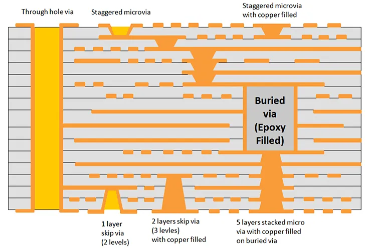
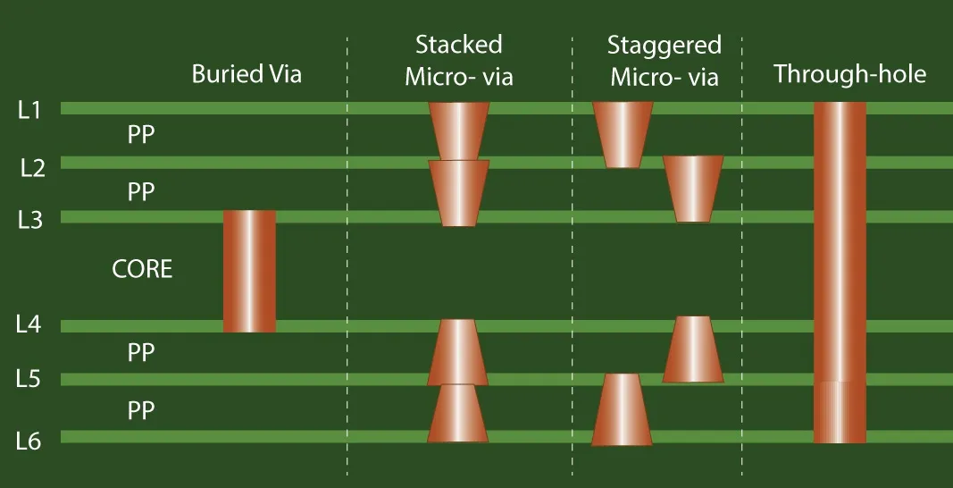
Controlled depth drilling refers to the precise formation of vias that stop at a predetermined depth within the PCB stackup, typically for blind or buried vias in HDI structures. Unlike through-hole drilling, which spans the full board thickness, this method targets specific interlayer connections, optimizing routing density and signal paths. In high-density PCB design, controlled depth microvias enable tighter spacing, finer lines, and reduced parasitic inductance, which are critical for high-speed signals.
The relevance of these techniques stems from the need to accommodate increasing component densities and miniaturization trends in electronics. HDI PCBs often feature multiple buildup layers, where microvias with diameters under conventional mechanical limits necessitate specialized drilling. Manufacturers rely on controlled depth drilling to avoid damaging inner layers, ensuring plating integrity and minimizing warpage during lamination. According to IPC-2226 guidelines, proper microvia design directly impacts yield and long-term reliability in advanced PCB manufacturing.
Furthermore, this approach supports staggered and stacked via configurations, common in any-layer HDI boards, enhancing overall board functionality without excessive layer counts. Factory insights reveal that inconsistent depth control leads to plating voids or breakout failures, underscoring the need for robust process controls from design through fabrication.
Technical Principles of Controlled Depth Drilling
Controlled depth drilling operates on principles of material removal tailored to the dielectric and copper properties in HDI stackups. Mechanical methods use high-speed spindles with depth-sensing feedback or entry/exit tabs to limit penetration, suitable for larger vias in outer layers. However, for microvias, limitations in bit size and aspect ratio restrict mechanical drilling, shifting focus to non-contact techniques like laser ablation.
Laser drilling HDI leverages photon energy to vaporize material selectively, with UV excimer lasers excelling at ablating copper and resin simultaneously for blind vias. CO2 lasers, operating at longer wavelengths, effectively drill dielectrics but require copper etch preprocessing to expose underlying material. The process involves pulse duration, fluence, and repetition rate to achieve tapered profiles that facilitate plating, preventing issues like carbon residue or heat-affected zones.
Plasma drilling represents an emerging plasma etching variant, using reactive gases to etch vias isotropically, offering uniformity in challenging materials. Depth control in all methods hinges on stackup calibration, where dielectric thickness dictates parameter sets to hit target endpoints precisely. These principles align with performance specifications in standards like IPC-6012DS, emphasizing via geometry tolerances for HDI qualification.
Thermal and photochemical ablation mechanisms differ fundamentally: UV lasers break molecular bonds for clean cuts, while CO2 induces melting and ejection. Factory calibration involves test coupons to verify depth uniformity across panels, accounting for material variations like resin content or glass transition temperature.
Advanced Techniques in HDI PCB Drilling
Advanced PCB manufacturing employs hybrid laser systems combining UV and CO2 for sequential drilling, first ablating copper with UV then dielectric with CO2, enhancing throughput for production volumes. Stacked microvia formation requires multiple lamination cycles, where each buildup layer undergoes controlled depth drilling post-outer layer processing. This sequential approach allows via-in-pad designs, critical for high-density PCB design with BGA footprints.
Plasma-assisted drilling addresses limitations in resin ablation, providing sidewall smoothness superior to pure laser methods, reducing electroless copper deposition challenges. Multi-beam laser arrays enable parallel processing, scaling for high-volume HDI fabrication while maintaining depth precision via real-time optical feedback. These techniques mitigate common issues like via flare or dog-boning through optimized beam profiles and assist gases.
In factory settings, adaptive control systems adjust parameters based on inline metrology, ensuring compliance across panel variations. For ultra-fine microvias, femtosecond lasers offer minimal heat input, preserving dielectric integrity in low-loss materials. Integration with direct imaging for drill fiducials further refines registration, supporting any-layer interconnects.
Best Practices for Controlled Depth Microvias in Production
Implementing best practices begins with stackup planning, specifying dielectric thicknesses compatible with drilling aspect ratios to avoid breakthrough risks. Pre-drill verification using pilot holes or X-ray laminography confirms layer alignment before full production. Parameter optimization, derived from design files, includes feed rates for mechanical and pulse energies for lasers, validated on scrap panels.
Post-drill desmear processes, such as plasma or chemical etching, remove residue to ensure plating adhesion, a step vital for HDI reliability. Sequential buildup demands intermediate inspections for via continuity and depth via cross-sectioning per IPC-2226 recommendations. Factory protocols emphasize cleanroom environments to prevent contamination, which exacerbates drill smear.
Yield enhancement comes from statistical process control, monitoring depth variation to stay within tolerances. Collaboration between design and manufacturing teams ensures drill files account for material shrinkage and registration offsets.
Challenges and Troubleshooting in HDI PCB Drilling
Common challenges include inconsistent depth due to material inhomogeneity or spindle runout in mechanical drilling, leading to open or shorted vias. Laser techniques face resin charring or copper splash, addressed by waveform tuning and vacuum extraction. Troubleshooting involves root cause analysis via optical and SEM inspection, correlating defects to process parameters.
Warpage from asymmetric buildup stresses vias, mitigated by carrier panels during lamination. Reliability testing simulates thermal cycling to detect electromigration in microvias. Factory insights stress proactive design rules, like pad-to-via spacing, to buffer tolerances.
Conclusion
Controlled depth drilling stands as a foundational technique in advanced PCB manufacturing for HDI PCBs, enabling the precision required for modern high-density designs. From laser drilling HDI to plasma alternatives, these methods deliver reliable microvia formation when guided by best practices and standards. Manufacturers achieve superior yields by integrating metrology and process controls, ensuring robust interconnects for demanding applications.
FAQs
Q1: What distinguishes controlled depth microvias from standard vias in HDI PCB drilling?
A1: Controlled depth microvias stop at specific layers, unlike through vias that span the full stackup, allowing denser routing in high-density PCB design. Factory processes use laser or mechanical methods with precise depth control to form blind or buried structures. This supports sequential lamination, aligning with IPC-2226 for optimal performance.
Q2: Why is laser drilling HDI preferred over mechanical drilling for advanced PCB manufacturing?
A2: Laser drilling HDI achieves smaller diameters and better depth precision in thin dielectrics, essential for microvias under mechanical limits. It minimizes mechanical stress and enables clean ablation through copper foils. Production benefits include higher throughput for stacked vias, though it requires desmear for plating readiness.
Q3: How do standards like IPC-6012DS influence controlled depth drilling practices?
A3: IPC-6012DS outlines qualification criteria for HDI via geometry and reliability, guiding depth tolerances and inspection. Factories use these specs to validate processes against performance benchmarks. Compliance ensures consistency in advanced PCB manufacturing, reducing field failures.
Q4: What are key troubleshooting steps for depth inconsistencies in HDI PCB drilling?
A4: Inspect stackup alignment and calibrate equipment parameters first, then analyze cross-sections for breakthrough. Adjust pulse energy or spindle depth based on findings. Inline metrology prevents panel-wide defects in production.


