 ALLPCB


Introduction
Flexible printed circuit boards, or flex PCBs, have revolutionized electronics design by enabling compact, lightweight interconnects in tight spaces. While thin flex PCBs excel in high-flex applications, there are scenarios where increasing the overall thickness proves advantageous. A thicker flex PCB balances flexibility with enhanced structural integrity, making it suitable for demanding environments. Engineers often face the decision of when to use a thicker PCB to optimize performance without sacrificing the core benefits of flex technology. This article explores thick flex PCB applications, the advantages of thicker flexible PCBs, and key considerations for implementation. Factory insights reveal that proper thickness selection aligns production with reliability goals.
What Is a Thick Flex PCB and Why Does It Matter?
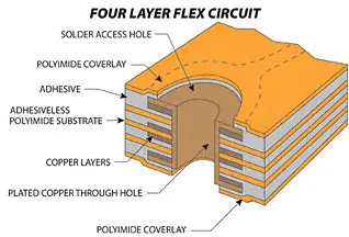
A thick flex PCB refers to a flexible circuit with increased material stackup, such as additional dielectric layers, heavier copper weights, or reinforced substrates compared to standard single-layer thin flex designs. These boards maintain bendability but offer greater rigidity in specific zones, typically through polyimide or adhesive builds that exceed minimal flex profiles. Thickness in flex PCBs directly influences mechanical handling, electrical performance, and thermal management during manufacturing and end-use. In factory settings, thicker constructions reduce handling damage and improve yield rates under IPC-6013 qualification criteria. This matters for electrical engineers specifying boards for vibration-prone or high-power assemblies, where thin flex might fail prematurely. Selecting the right thickness ensures compliance with performance specs while minimizing rework.
Technical Principles of Thickness in Flex PCBs
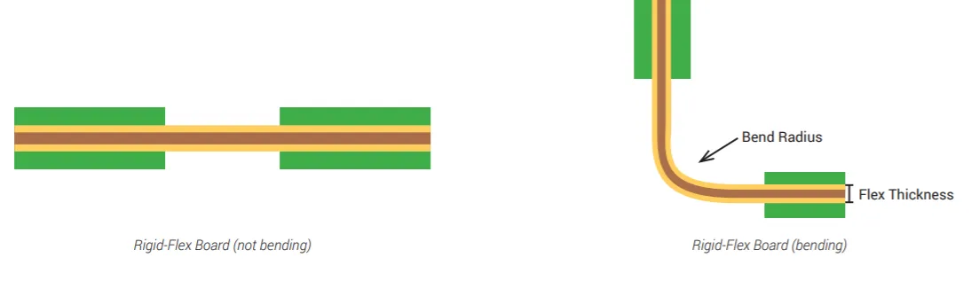
The core principle governing flex PCB thickness revolves around the bend radius formula, where greater thickness demands a larger minimum bend to avoid stress concentrations in copper traces. Thicker dielectrics distribute mechanical strain more evenly, reducing fatigue cracks during repeated flexing. Electrically, increased copper thickness lowers resistance and supports higher current densities without excessive heating. Thermally, bulkier materials enhance heat dissipation paths, critical in multilayer stackups. Manufacturing processes like lamination and etching must account for these dynamics to prevent delamination, as outlined in design standards. Engineers benefit from modeling these interactions early to predict long-term reliability.
In dynamic applications, thicker flex PCBs exhibit superior resistance to cyclic bending fatigue because the neutral axis shifts favorably within the stackup. This configuration minimizes trace elongation on outer layers. Vibration resistance improves as thickness adds damping, absorbing energy that thin boards transmit directly. Signal integrity benefits from controlled impedance in thicker dielectrics, reducing crosstalk in high-speed signals. Factory testing validates these principles through peel strength and flex endurance evaluations.
Advantages of Thicker Flexible PCBs
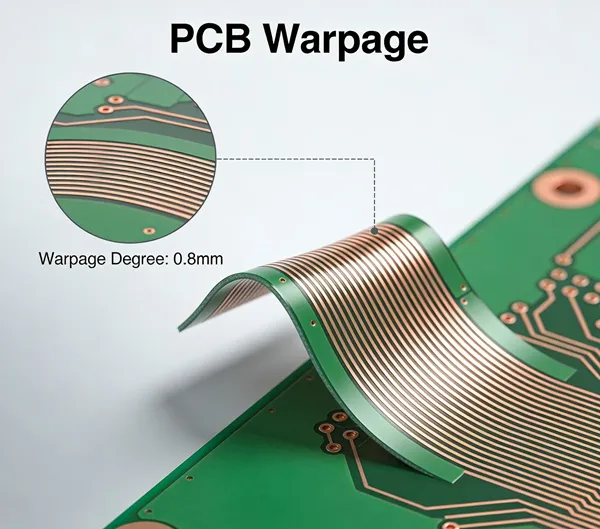
Thicker flexible PCBs provide several key advantages that make them preferable in select designs. First, they offer enhanced mechanical durability, resisting tears, punctures, and warpage better than thin counterparts during assembly and operation. This is particularly valuable in automated pick-and-place processes where boards endure handling stresses. Second, thicker constructions support heavier copper foils, enabling higher current-carrying capacity for power distribution circuits. Electrical losses decrease, improving efficiency in compact power modules.
Third, thermal performance elevates with greater material volume acting as a heat sink, aiding component longevity in elevated temperature environments. Thicker boards also simplify stiffener integration, reducing overall assembly steps. From a factory perspective, these advantages translate to higher first-pass yields and fewer field failures. Vibration-prone setups gain stability without rigid reinforcements. Overall, the advantages of thicker flexible PCBs justify their use when flexibility is secondary to robustness.
When to Use a Thicker PCB: Key Scenarios and Applications
Engineers should opt for a thicker PCB when the design prioritizes durability over extreme bendability, such as in semi-rigid interconnects within enclosures. Thick flex PCB applications shine in automotive sensor harnesses, where constant vibration demands robust traces. Aerospace controls benefit from the added puncture resistance against debris or impacts. Medical devices with moving parts, like robotic endoscopes, leverage thickness for repeated flex cycles without degradation.
High-power LED drivers or battery management systems require thicker copper for current handling, making thick flex ideal. In consumer wearables with larger batteries, thickness prevents sagging under component weight. Factory data shows these applications achieve better conformance to reliability tests when thickness matches stress profiles. Hybrid rigid-flex transitions also favor thicker flex tails for seamless mating. Ultimately, when to use a thicker PCB hinges on balancing flex needs with mechanical and electrical loads.
- High dynamic bending: Thin flex preference: Consumer displays; Thick flex preference: Automotive harnesses
- Low power signals: Thin flex preference: Smartphones; Thick flex preference: Power modules
- Extreme miniaturization: Thin flex preference: Hearing aids; Thick flex preference: Industrial sensors
- Vibration exposure: Thin flex preference: Static wearables; Thick flex preference: Aerospace controls
Best Practices for Designing and Manufacturing Thicker Flex PCBs
Start with stackup simulation to verify bend radii per IPC-2223 guidelines, ensuring trace widths accommodate thickness-induced impedance shifts. Specify coverlay and adhesive thicknesses to maintain uniformity, avoiding voids during lamination. Incorporate tear stops and anchor points at bend zones to enhance integrity. Factory lamination uses controlled pressure to bond thicker builds without wrinkles.
Testing protocols include cyclic flexing and thermal shock to validate performance. Select polyimide for its thermal stability in thicker formats. Collaborate with manufacturers early on panelization, as thicker boards affect throughput. Post-etch annealing relieves stresses inherent in heavy copper. These practices ensure production scalability and field reliability.
Insights from Manufacturing: Common Challenges and Solutions
In production, thicker flex PCBs can exhibit higher warpage post-lamination due to differential shrinkage, addressed by symmetric stackups and bake cycles. Solder mask adhesion improves with plasma treatment on thicker surfaces. Handling thicker tails requires adjusted fixturing to prevent creasing. Real-world assemblies in vibration tests show thicker designs outlasting thin ones by distributing stresses effectively.
Engineers troubleshooting delamination find root causes in mismatched CTE materials, resolved by qualified adhesives. Impedance mismatches in high-speed thicker flexes demand precise etch control. Factory yields optimize with inline optical inspection tailored to thickness variations. These insights guide specifiers toward robust outcomes.
Conclusion
Thicker flex PCBs represent a strategic choice when applications demand more than just flexibility. The advantages of thicker flexible PCBs, from mechanical strength to thermal resilience, make them essential in high-reliability sectors. Thick flex PCB applications underscore their value in bridging thin flex limitations without full rigid transitions. Adhering to standards like IPC-6013 ensures manufacturability. Electrical engineers gain confidence by evaluating thickness against specific loads early in design. Ultimately, thickening up enhances overall system performance and longevity.
FAQs
Q1: What are the main thick flex PCB applications?
A1: Thick flex PCB applications include automotive sensors, aerospace interconnects, and medical robotics where vibration and mechanical stress prevail. These scenarios benefit from enhanced durability while retaining routing flexibility. Factory production aligns with IPC-6013 for qualification, ensuring reliability in dynamic environments. Engineers select thicker builds for power handling in battery systems too.
Q2: What are the advantages of thicker flexible PCBs?
A2: Advantages of thicker flexible PCBs encompass superior mechanical resistance, higher current capacity, and improved thermal dissipation. They reduce warpage risks and simplify assembly stiffening. In manufacturing, thicker designs yield better handling tolerance and vibration damping. This makes them ideal when extreme thinness compromises longevity.
Q3: When to use a thicker PCB in flex designs?
A3: Use a thicker PCB when designs face high vibration, power demands, or handling stresses exceeding thin flex limits. Applications like industrial controls or wearables with batteries favor this approach. Per IPC-2223, verify bend compatibility first. Factory insights confirm reduced failures in semi-dynamic uses.
Q4: How does thickness impact flex PCB performance?
A4: Thickness increases bend radius needs but boosts fatigue life and signal integrity. Thicker copper lowers resistance, aiding high-current paths. Thermal management improves with added material mass. Standards guide balanced specs for optimal factory output.
References
IPC-6013 - Qualification and Performance Specification for Flexible and Rigid-Flex Printed Boards. IPC
IPC-2223 - Sectional Design Standard for Flexible Printed Boards. IPC
IPC-A-610 - Acceptability of Electronic Assemblies. IPC





