 ALLPCB


Introduction
In modern PCB assembly, designs increasingly incorporate components with varying heights, such as tall inductors alongside fine-pitch ball grid arrays (BGAs) and quad flat no-leads (QFNs). This mix creates challenges during solder paste printing, where a uniform stencil thickness often leads to defects like insufficient paste volume for taller parts or bridging on smaller ones. Step stencils address these issues by providing multi-level thicknesses tailored to component needs, enabling precise solder paste volume control. Engineers benefit from reduced rework and higher yields when implementing step stencil design effectively. This article explores the principles, best practices, and troubleshooting for step stencils in mixed-component PCBs, drawing on practical assembly insights.
What Are Step Stencils?
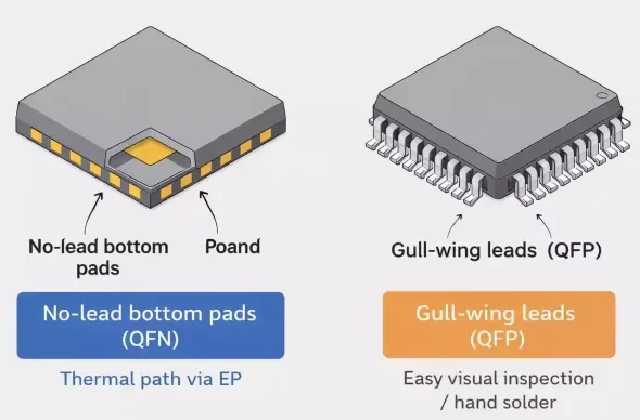
Step stencils, also known as multi-level stencils, feature areas of different thicknesses within the same stencil frame to accommodate components of varying heights. Thinner sections support fine-pitch devices like QFNs and BGAs, minimizing solder bridging and excess paste, while thicker regions supply adequate volume for taller components such as inductors or connectors. These stencils can be step-up, where thicker material rises above the base, or step-down, where areas are etched thinner. Manufacturing typically involves laser cutting or etching stainless steel foil, followed by welding or electroforming for multi-level features. In pin-in-paste applications, step stencils deposit extra paste around through-hole pins, facilitating reliable mechanical and electrical joints during reflow.
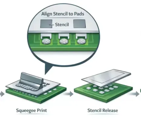
The design allows the squeegee blade to contact the entire surface uniformly during printing, ensuring consistent transfer. Without step stencils, engineers often resort to multiple printing passes or manual paste addition, increasing cycle time and defect risks. IPC-7525 provides guidelines for such stencil fabrication, emphasizing aperture quality and step integrity.
Why Step Stencils Matter for Mixed-Component PCBs
Mixed-component PCBs are common in applications like power supplies, automotive electronics, and telecommunications, where space constraints demand integrating large passives with high-density ICs. Uniform stencils fail here because fine-pitch parts require thin apertures (typically 100-125 microns) for clean release, while tall components need 150-200 microns or more for sufficient solder joints. Step stencils optimize solder paste volume control, preventing issues like tombstoning on small chips or cold joints on larger parts. They reduce solder defects by up to significant margins in high-volume production, streamlining the surface mount technology (SMT) process.
Varying component height stencils also support hybrid assemblies, combining SMT and through-hole elements without separate stencils. This approach cuts material costs and setup times, critical for prototyping and low-volume runs. In troubleshooting scenarios, step stencils prove invaluable when board warpage or component tolerances vary, maintaining paste height consistency across the panel.
Technical Principles of Step Stencil Design
Step stencil design hinges on aperture geometry, thickness transitions, and material properties to ensure reliable solder paste deposition. Aperture walls must be vertical and smooth, with an area ratio (open area to wall area) above 0.6 for optimal paste release, as guided by industry guidelines. Thicker steps for tall components increase paste volume proportionally to standoff height, while thinner areas for BGAs and QFNs control fillet size and prevent bridging. Laser-cut stencils offer precision down to 20-micron features, essential for 0.3mm pitch devices.
Multi-level transitions require careful placement to avoid stress points during printing; steps should align with fiducials for registration accuracy. In pin-in-paste stencil designs, apertures around pins are enlarged and thickened to allow paste flow into holes without starving adjacent SMT pads. J-STD-005 outlines solder paste requirements that complement these designs, ensuring viscosity and particle size suit varying thicknesses. Engineers must simulate paste flow using software to predict release behavior before fabrication.
For QFN stencil optimization, U-shaped or scooped apertures in thinner sections promote void-free underfill during reflow. BGA stencil apertures often incorporate home-plate shapes to direct paste under the package, reducing the risk of head-in-pillow defects.
Related Reading: Step Stencil vs. Standard Stencil: Which is Right for Your PCB?
Best Practices for Implementing Step Stencils
Start with land pattern design per IPC-7351 principles, ensuring pads match the intended paste volume for each component type. Specify step heights based on component datasheets: thin (0.1mm) for 01005 passives and 0.4mm pitch QFNs, medium (0.125-0.15mm) for BGAs, and thick (0.2mm+) for inductors over 1mm tall. Use fiducial marks at step boundaries for alignment, and incorporate relief pockets to prevent paste buildup at transitions. During fabrication, opt for nickel plating on steps to enhance release and durability.
Printing parameters demand adjustment: slower squeegee speeds (20-40mm/s) for thick areas, and pressure around 1-2kg to avoid stencil damage. Clean stencils every 5-10 prints with targeted under-stencil wipes, focusing on step edges. Validate volume control with SPI (solder paste inspection) metrology, targeting 100-120% of nominal height for tall parts and 80-100% for fine-pitch.
For pin-in-paste stencils, position pins precisely within thickened paste islands, ensuring 50-75% hole fill post-print. Test panels reveal if steps cause uneven pressure; iterate by adjusting bevel angles at transitions.
Troubleshooting Step Stencil Issues in Assembly
Common defects trace back to poor step integrity or mismatched paste rheology. Insufficient paste on tall components signals too-thin steps or low squeegee pressure; measure heights with laser profilometry and adjust. Bridging on QFNs or BGAs often stems from thick apertures or dirty stencils; reduce thickness or add trapezoidal walls. If steps delaminate after cycles, verify weld strength during incoming inspection.
Warpage exacerbates issues in mixed assemblies; use localized thinning to compensate for board bow. Pin-in-paste failures like incomplete hole fill require larger apertures or multiple prints. IPC J-STD-001 criteria for soldered joints help diagnose reflow problems linked to paste volume variability. Log print yields and correlate with step locations for data-driven fixes.
Related Reading: The Ultimate Guide to Step Stencil Manufacturing: Processes and Materials
Conclusion
Step stencils revolutionize solder paste deposition for mixed-component PCBs by enabling precise volume control across varying heights. From multi-level designs for BGAs and QFNs to pin-in-paste solutions, they minimize defects and boost efficiency. Adhering to best practices in design, printing, and troubleshooting ensures reliable assembly outcomes. Electric engineers should integrate step stencil design early in the process for optimal results, leveraging standards like IPC-7525 for guidance.
FAQs
Q1: What is step stencil design, and when should it be used?
A1: Step stencil design creates multi-level thicknesses to match varying component heights on PCBs, ideal for boards with fine-pitch QFNs next to tall inductors. Use it when uniform stencils cause paste volume imbalances, leading to bridging or insufficient joints. This approach simplifies printing and reduces rework, aligning with SMT best practices for mixed assemblies. Always verify with SPI post-print.
Q2: How does a multi-level stencil improve solder paste volume control?
A2: A multi-level stencil, or step stencil, applies thicker paste to tall components while using thin sections for fine-pitch parts like BGAs, preventing excess or deficit. It maintains uniform squeegee contact, ensuring consistent deposition. Troubleshoot by checking area ratios and paste viscosity per J-STD-005. This controls fillet sizes effectively in high-density boards.
Q3: What are the benefits of pin-in-paste stencils for through-hole components?
A3: Pin-in-paste stencils deposit extra solder volume around through-hole pins using thickened apertures, enabling reflow soldering without wave processes. This suits mixed SMT/TH assemblies, reducing handling steps. Ensure apertures allow paste flow without starving pads; inspect for 50-75% hole fill. It enhances mechanical strength in varying component height scenarios.
Q4: How to optimize BGA and QFN stencil apertures in step designs?
A4: For BGA and QFN stencils, use thinner steps with shaped apertures like home-plates to direct paste and minimize voids. Maintain vertical walls for clean release, targeting precise volumes per IPC-7525 guidelines. Troubleshoot bridging by reducing thickness or adding scoops. This ensures reliable under-package joints in mixed PCBs.
References
IPC-7525C - Stencil Design Guidelines. IPC
J-STD-005A - Requirements for Soldering Pastes. IPC/JEDEC, 2012
IPC J-STD-001 - Requirements for Soldered Electrical and Electronic Assemblies. IPC


