If you're searching for a comprehensive overview of the step stencil manufacturing process, you've come to the right place. Step stencils are critical tools in surface mount technology (SMT) for applying solder paste to printed circuit boards (PCBs) with precision, especially when components of varying sizes require different paste volumes. This guide will dive deep into the processes like laser cutting and chemical etching, explore common stencil materials such as stainless steel, and provide actionable insights for engineers and manufacturers. Let’s explore everything you need to know to optimize your stencil production and achieve flawless PCB assembly.
What Are Step Stencils and Why Are They Important?
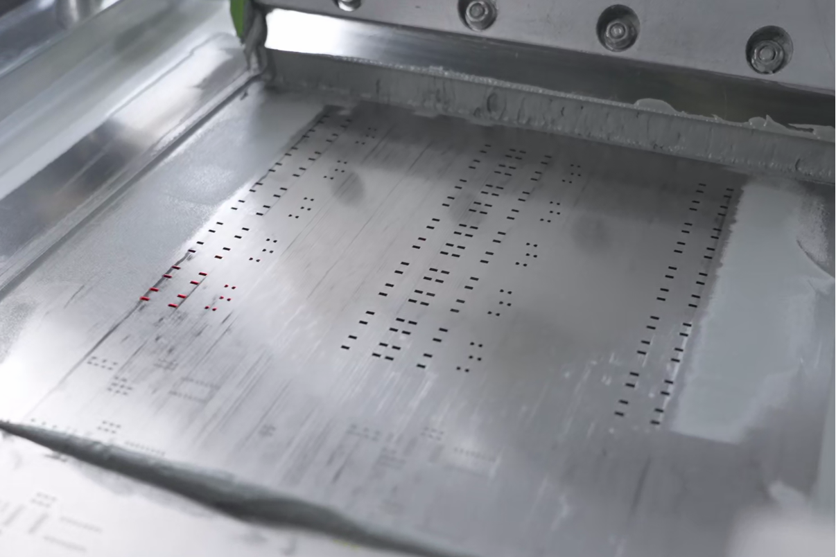
Step stencils are specialized tools used in SMT assembly to control the volume of solder paste applied to PCBs. Unlike standard stencils with uniform thickness, step stencils feature varying thicknesses—thicker areas for larger components needing more solder paste and thinner areas for smaller components requiring less. This design ensures precise paste deposition, reducing defects like insufficient solder or bridging.
In modern electronics, where components are shrinking and PCBs are becoming more complex, step stencils are essential for high-quality assembly. They address the challenge of mixed-component boards, ensuring reliability in applications from consumer gadgets to industrial systems. Understanding the step stencil manufacturing process is key to selecting the right stencil for your project and achieving consistent results.
Key Processes in Step Stencil Manufacturing
The creation of step stencils involves advanced techniques to achieve the necessary precision and durability. The two primary methods are laser cutting and chemical etching, often used in combination to produce high-quality stencils. Below, we break down these processes and their roles in stencil production.
Laser Cutting in Step Stencil Manufacturing
Laser cutting is a widely used method for creating the apertures (openings) in step stencils where solder paste is applied. This process uses a focused laser beam to cut through the stencil material, typically stainless steel, with extreme accuracy. Laser cutting is known for its ability to produce clean, precise openings, even for fine-pitch components with pad spacing as small as 0.4 mm or less.
Advantages of Laser Cutting:
- High Precision: Laser cutting achieves tolerances as tight as ±5 μm, ensuring accurate aperture placement.
- Consistency: The process is computer-controlled, minimizing human error and producing uniform results across large batches.
- Versatility: It can handle intricate designs and small features required for modern PCBs.
- Clean Edges: Laser-cut apertures often have a slight taper (trapezoidal shape), which aids in paste release during printing.
Limitations:
- Speed: Laser cutting can be slower compared to other methods, especially for larger stencils or complex step designs.
- Cost: The equipment and maintenance for laser cutting systems can be expensive, though the precision often justifies the investment.
In the step stencil manufacturing process, laser cutting is typically used for creating the final apertures after the stencil’s stepped structure is formed. This ensures the openings are precise, even in areas of varying thickness.
Chemical Etching for Step Stencil Production
Chemical etching is another critical process, often used to create the stepped regions of a stencil before laser cutting. This method involves applying a chemical solution, typically an acid, to selectively remove material from the stencil surface, creating areas of reduced thickness. Etching is ideal for forming large recessed areas or steps where thicker solder deposits are not needed.
Advantages of Chemical Etching:
- Cost-Effective for Steps: Etching can quickly create large stepped areas without the need for slow, point-by-point laser processing.
- Uniform Depth: It can achieve consistent thickness reduction across wide areas, with depth control down to 0.05 mm.
- Speed: For creating steps, etching is often faster than milling or repeated laser passes.
Limitations:
- Lower Precision: Etching is less accurate than laser cutting for fine details, often resulting in slight undercuts or uneven edges.
- Environmental Impact: The chemicals used in etching require careful handling and disposal, posing environmental challenges.
- Not Ideal for Apertures: Etched openings can form a “sandglass” shape, making them unsuitable for precise solder paste application.
In step stencil production, chemical etching is typically performed first to create the thickness variations, followed by laser cutting to define the apertures. This hybrid approach combines the strengths of both methods for optimal results.
Combining Laser Cutting and Chemical Etching
Most high-quality step stencils are manufactured using a combination of chemical etching and laser cutting. Etching forms the stepped structure by reducing thickness in specific areas, while laser cutting ensures precise apertures for solder paste deposition. This dual-process approach allows manufacturers to balance cost, speed, and accuracy.
For example, a stencil might start as a 0.15 mm thick sheet of stainless steel. Chemical etching reduces certain areas to 0.10 mm for fine-pitch components, while the thicker 0.15 mm areas remain for larger components. Laser cutting then creates the apertures with exact dimensions, ensuring paste volume control with tolerances as tight as ±10 μm.
Stencil Materials: Why Stainless Steel Dominates
The choice of stencil materials plays a huge role in the performance and durability of step stencils. While various materials have been used over the years, stainless steel remains the industry standard for several reasons. Let’s explore why this material is the go-to choice and touch on alternative options.
Stainless Steel Stencils: The Industry Standard
Stainless steel stencils are the most popular choice for step stencil manufacturing due to their durability, precision, and compatibility with modern processes like laser cutting and chemical etching. Typically, grades like 304 or 301 stainless steel are used, offering a balance of strength and corrosion resistance.
Benefits of Stainless Steel:
- Durability: Stainless steel can withstand thousands of print cycles without deforming, making it ideal for high-volume production. Some stencils last for over 50,000 prints with proper care.
- Corrosion Resistance: It resists rust and chemical degradation, even when exposed to solder paste and cleaning solvents.
- Precision Compatibility: Stainless steel works well with laser cutting, allowing for clean, accurate apertures as small as 0.2 mm in diameter.
- Thermal Stability: It maintains its shape under temperature fluctuations during SMT processes, ensuring consistent performance.
Drawbacks:
- Cost: Stainless steel is more expensive than alternatives like plastic or nickel, though its longevity often offsets the initial investment.
- Weight: It’s heavier than some materials, which can be a minor inconvenience during handling.
For most SMT applications, the advantages of stainless steel stencils far outweigh the drawbacks, making them the preferred choice for step stencil manufacturing.
Alternative Stencil Materials
While stainless steel dominates, other materials are sometimes used for specific applications or cost considerations. These include:
- Nickel: Nickel stencils offer excellent paste release due to their smooth surface and are often used for ultra-fine pitch applications. However, they are less durable than stainless steel, with a shorter lifespan of around 20,000 prints.
- Polyimide (Plastic): Lightweight and inexpensive, polyimide stencils are suitable for low-volume or prototype runs. They lack the durability for high-volume production, often deforming after just a few hundred prints.
For step stencils, where precision and durability are critical, stainless steel remains the best choice in most cases. Alternatives may be considered for niche or budget-constrained projects.
Step Stencil Design Considerations
Beyond manufacturing processes and materials, designing a step stencil requires careful planning to ensure optimal performance. Here are some key factors to consider during the step stencil manufacturing process.
Thickness Variations
Step stencils typically range from 0.08 mm to 0.2 mm in thickness, with steps as small as 0.02 mm in height. The thickness must match the solder paste volume needs of each component. For instance, a fine-pitch QFP might require a 0.1 mm thick area, while a larger connector needs 0.15 mm for adequate paste.
Aperture Design
Aperture size and shape directly impact solder paste deposition. Laser-cut apertures often have a slight taper (1-2 degrees), aiding paste release. The area ratio—aperture opening to wall thickness—should ideally be above 0.66 to prevent clogging.
Step Placement
Steps should be strategically placed to avoid stress points that could cause stencil deformation. A minimum distance of 1.5 mm between step transitions helps maintain structural integrity during printing.
Benefits of Using Step Stencils in SMT Assembly
Step stencils offer several advantages over traditional single-thickness stencils, making them indispensable for modern PCB assembly:
- Optimized Solder Volume: They allow precise control over paste volume, reducing defects by up to 30% in mixed-component boards.
- Improved Yield: By tailoring thickness to component needs, step stencils enhance first-pass yield rates, often exceeding 95% in well-designed processes.
- Versatility: They accommodate a wide range of component sizes on a single board, streamlining assembly for complex designs.
Challenges in Step Stencil Manufacturing
Despite their benefits, step stencils come with manufacturing challenges:
- Complexity: Creating precise steps and apertures requires advanced equipment and expertise, increasing production time.
- Cost: The combined use of chemical etching and laser cutting can raise costs by 20-40% compared to standard stencils.
- Maintenance: Step stencils require careful cleaning to prevent paste buildup in recessed areas, which can reduce lifespan if not managed properly.
How to Choose the Right Step Stencil for Your Project
Selecting the right step stencil involves evaluating your PCB design and production needs. Consider the following:
- Component Mix: Assess the range of component sizes on your board to determine the number and depth of steps needed.
- Production Volume: For high-volume runs, invest in durable stainless steel stencils to ensure longevity.
- Budget: Balance the upfront cost of advanced manufacturing processes with the long-term benefits of reduced defects and higher yields.
- Manufacturer Expertise: Partner with a provider experienced in both laser cutting and chemical etching to guarantee precision.
Conclusion: Mastering Step Stencil Manufacturing
Step stencils are a game-changer in SMT assembly, offering unmatched control over solder paste application for complex PCB designs. By understanding the step stencil manufacturing process, including techniques like laser cutting and chemical etching, and selecting the right stencil materials such as stainless steel, you can significantly improve your assembly outcomes. Whether you're dealing with fine-pitch components or large connectors, step stencils provide the precision and versatility needed for today’s electronics.
At ALLPCB, we’re committed to supporting your PCB assembly needs with high-quality step stencils tailored to your specifications. By leveraging advanced manufacturing processes and durable materials, we help you achieve flawless results in every project. Dive into the world of step stencils and elevate your production process with the insights from this guide.
 ALLPCB


