 ALLPCB


Introduction
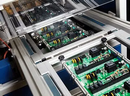
Complex printed circuit boards often feature a mix of surface-mount technology components and through-hole parts, presenting unique assembly challenges. Traditional methods like full wave soldering can damage sensitive surface-mount devices, while reflow soldering alone struggles with larger through-hole connectors. Selective soldering with stencil printing emerges as a hybrid solution, enabling precise solder paste application for reflow-compatible parts followed by targeted soldering for the rest. This approach minimizes defects, enhances reliability, and supports high-density designs common in modern electronics. By integrating these processes, engineers achieve better control over solder joints in mixed-technology assemblies. The result is improved yield and compliance with industry requirements for robust PCB assembly.
Understanding Stencil Printing in PCB Assembly
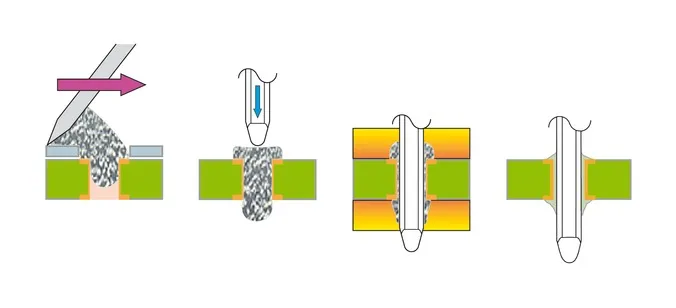
Stencil printing involves using a thin metal foil with laser-cut apertures aligned over PCB pads to deposit solder paste accurately. The paste, a mixture of solder particles and flux, transfers through the stencil via a squeegee blade under controlled pressure and speed. This method ensures uniform volume and placement, critical for surface-mount reflow. For complex boards, stencils can also accommodate solder paste application for through-hole components through techniques like pin-in-paste, where paste fills vias partially. Proper stencil thickness, typically between 0.1 and 0.15 mm, balances release efficiency and paste volume. Alignment fiducials on both stencil and board prevent misalignment, which could lead to bridging or insufficient solder.
Industry guidelines such as IPC-7525 outline stencil design parameters, including aspect and area ratios, to optimize paste transfer. Engineers must consider pad size and pitch when designing apertures, often reducing them slightly for better release. Printing parameters like snap-off distance and squeegee angle further refine the process. Inspection post-printing verifies volume using spirometry or laser profiling. This foundational step sets the stage for subsequent reflow, directly impacting joint quality.
The Role of Selective Soldering for Through-Hole Components
Selective soldering targets specific through-hole joints using a localized molten solder pot, avoiding exposure of the entire board to heat. A fluxer applies flux precisely, followed by preheating to activate flux and prevent thermal shock. The solder nozzle then wets the leads and pads, forming reliable fillet joints. This method suits components like large connectors or heat sinks that cannot withstand reflow temperatures. Drop-jet fluxing and infrared preheaters enhance precision on densely populated boards. Post-soldering cleaning removes flux residues to prevent corrosion.
Unlike wave soldering, selective soldering reduces shadowing effects where one lead blocks solder flow to others. It excels in low-to-medium volume production for complex geometries. Process parameters include solder temperature around 250-260°C and immersion time of 3-5 seconds per joint. Nitrogen atmospheres minimize dross and oxidation. Combining this with prior stencil printing allows reflow of surface-mount parts first, preserving their integrity.
Why Combine Stencil Printing and Selective Soldering?
Complex PCBs demand efficiency without compromising quality, and selective soldering with stencil printing addresses this by segmenting the assembly. Stencil printing handles high-density surface-mount and select through-hole via pin-in-paste, enabling a single reflow step. Remaining through-hole parts, intolerant to reflow, undergo selective soldering afterward. This hybrid reduces handling, cuts cycle time, and lowers defect rates from thermal stress. It supports combining stencil printing and wave soldering variants, though selective offers superior precision for fine-pitch areas.
For engineers, this approach aligns with mixed-technology realities in automotive, aerospace, and telecom boards. It avoids glue dots for bottom-side surface-mount, simplifying logistics. Yield improvements stem from controlled paste volume and targeted heat application. Troubleshooting becomes straightforward, as issues isolate to specific process stages. Overall, it boosts manufacturability for boards exceeding traditional process limits.
Related Reading: Mastering Selective Soldering: A Comprehensive Guide for PCB Assembly
Technical Principles of the Combined Process
The synergy begins with stencil design per IPC-7525, where apertures for through-hole pads extend into the hole for paste intrusion. Aspect ratio (aperture width over thickness) should exceed 1.5 for clean release, while area ratio (aperture area over wall area) targets above 0.66. Paste rheology influences fill depth in vias, typically 50-75% for reliable reflow joints. After printing and component placement, reflow melts the paste, forming intermetallic bonds.
Post-reflow, selective soldering flux must be compatible with reflow residues, often no-clean types. Preheat profiles ramp to 150°C to equalize temperatures, preventing voids. Solder wave dynamics ensure wetting without bridging, governed by capillary action and surface tension. Nitrogen purging reduces oxides, improving fillet formation. Thermal profiling monitors the entire sequence to avoid exceeding component limits.
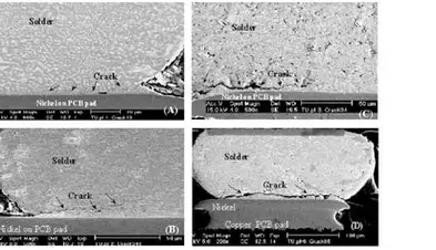
Joint integrity follows IPC-A-610 criteria, assessing fillet height, wetting, and voids. For solder paste application for through-hole components, stencil thickness adjusts to achieve adequate volume post-reflow. Simulations via software predict paste flow, aiding design iteration. This technical foundation ensures repeatability across production runs.
Related Reading: Understanding Stencil Printing: A Comprehensive Guide for SMT Assembly
Best Practices for Implementation
Start with dual-stencil strategies: one for fine-pitch surface-mount, another stepped for through-hole. Validate printing with AOI for paste defects like insufficient deposit or smearing. Optimize reflow profiles with peak temperatures 20-30°C above liquidus, holding 60-90 seconds. For selective soldering, program nozzle paths to minimize drag-out, using flux quantities of 1-2 mg per joint.
Fixturing secures boards during selective soldering, accommodating warpage. Cleanliness checks post-process use ion chromatography for residues. Process control charts track key variables like paste height and joint appearance. Training operators on visual criteria per standards prevents human error. For high-mix production, quick-change tooling accelerates setups.
Trial runs on prototypes refine parameters, correlating to reliability tests like thermal cycling. Document deviations for continuous improvement. This systematic approach maximizes the benefits of selective soldering with stencil printing.
Troubleshooting Common Challenges
Bridging in stencil printing often traces to excessive paste volume or poor snap-off; reduce aperture size or adjust squeegee pressure. Insufficient hole fill in pin-in-paste results from high stencil thickness; thin to 0.1 mm and use Type 4 paste. Post-reflow, tombstoning affects small chips; balance thermal mass via profile tweaks.
In selective soldering, poor wetting signals flux issues; verify activation temperature. Solder balls arise from turbulence; lower immersion speed. Thermal damage to nearby surface-mount manifests as delamination; extend preheat zones. Use X-ray for void inspection and cross-sectioning for fillet analysis. Systematic root-cause analysis, like fishbone diagrams, resolves recurrences efficiently.
Case Study: High-Density Telecom Board
A telecom module with 80% surface-mount and 20% through-hole relays used this combined method. Stencil printing applied paste to all reflowable parts, including pin-in-paste for low-profile TH. Reflow yielded 99% first-pass for surface-mount. Selective soldering completed relays with zero rework. Cycle time dropped 25%, defects fell below 100 ppm. This validated the approach for volume production.
Conclusion
Combining stencil printing and selective soldering optimizes complex PCB assembly by leveraging each process's strengths. Precise paste application enables efficient reflow for most components, while targeted soldering handles the rest reliably. Adhering to standards ensures quality joints and process robustness. Engineers gain flexibility for evolving designs, reducing costs and enhancing performance. This method future-proofs mixed-technology production against density increases.
FAQs
Q1: What are the benefits of selective soldering with stencil printing for mixed PCBs?
A1: This combination allows reflow soldering of surface-mount and select through-hole via pin-in-paste, followed by precise selective soldering for heat-sensitive parts. It minimizes thermal damage, improves yield, and supports high-density layouts. Process control is enhanced, with defects isolated to stages. Overall, it streamlines assembly for complex boards.
Q2: How does solder paste application for through-hole components work with stencils?
A2: Stencils feature apertures that deposit paste around and into through-hole pads, achieving partial via fill for reflow. Design per IPC-7525 ensures adequate volume post-melt. This pin-in-paste technique forms reliable joints without secondary soldering for compatible parts. Validation via inspection prevents voids.
Q3: When to choose combining stencil printing and wave soldering over selective?
A3: Use this for bottom-side through-hole dominant boards post-top reflow, where volume justifies wave pallets. Selective suits sparse, precise TH on dense SMT. Wave risks shadowing; selective avoids it. Evaluate based on component count and geometry.
Q4: What IPC standards guide stencil printing in hybrid processes?
A4: IPC-7525 provides stencil design rules for paste printing, including mixed tech. IPC-A-610 defines joint acceptability. Follow for aspect ratios and inspection. These ensure consistency across reflow and selective stages.


