 ALLPCB


Introduction
Surface mount technology (SMT) assembly demands precision at every step, with solder paste deposition setting the foundation for reliable joints. A well-designed stencil ensures accurate paste volume and placement, directly impacting yield and defect rates. Poor stencil design often leads to issues like bridging, insufficient solder, or tombstoning, which can cascade through reflow and inspection. This article explores SMT stencil design guidelines, focusing on solder paste deposition accuracy, aperture size for SMT, stencil thickness selection, and strategies for optimizing SMT assembly. Engineers can apply these principles to troubleshoot real-world challenges and achieve consistent results. By adhering to established standards, assemblies gain robustness against process variations.
What Is SMT Stencil Design and Why It Matters
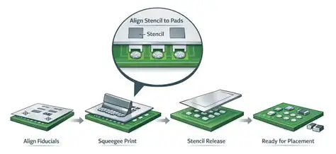
An SMT stencil is a thin metal foil, typically stainless steel, laser-cut with precise apertures aligned to PCB pads for solder paste transfer. During printing, a squeegee blade forces paste through these openings, depositing controlled volumes onto pads. Stencil design encompasses aperture geometry, thickness, and surface treatments to optimize release and minimize defects. It matters because solder paste deposition accuracy determines joint formation, electrical reliability, and overall assembly yield. In high-density boards with fine-pitch components, suboptimal designs amplify risks like solder balls or voids. Following SMT stencil design guidelines prevents these issues, ensuring scalability from prototypes to production.
Effective stencil design aligns with component land patterns and paste rheology, balancing volume needs across diverse parts. For instance, larger components require more paste for fillet formation, while fine-pitch parts prioritize clean release to avoid bridging. Engineers must consider the interplay of stencil parameters with reflow profiles and board warpage. Neglecting these factors leads to rework costs and reliability failures in the field. Ultimately, mastering stencil design elevates SMT assembly from acceptable to exceptional.
Fundamental Principles: Aspect Ratio and Area Ratio
Aspect ratio and area ratio govern solder paste release from stencil apertures, critical for deposition accuracy. Aspect ratio is the smallest aperture width divided by stencil thickness; IPC-7525C recommends a minimum of 1.5 for reliable printing, with 1.7 or higher ideal for challenging pastes. Lower values cause paste to cling to walls, resulting in insufficient deposits or stringing. Area ratio, calculated as aperture area divided by total wall contact area, should exceed 0.66 to promote clean lift-off. These metrics ensure paste transfer efficiency above 75-85%, varying with alloy type. Engineers calculate them early in design to flag risky apertures.
For rectangular apertures, area ratio uses the formula (length × width) / [2 × (length + width) × thickness]. Circular apertures simplify to diameter / (4 × thickness). Tools verify compliance across all features, prioritizing the smallest ones. Deviations demand thinner stencils or shape adjustments. These principles, rooted in IPC-7525C, form the backbone of SMT stencil design guidelines.
Related Reading: Solder Paste Stencil Design: Key Factors for Perfect PCB Printing
Stencil Thickness Selection for Optimal Performance
Stencil thickness directly influences paste volume and print definition, requiring careful selection based on finest-pitch components. IPC-7525C provides recommendations: 0.150-0.200 mm for pitches above 0.65 mm, 0.100-0.125 mm for 0.4-0.5 mm pitches, and 0.075-0.100 mm for ultra-fine below 0.4 mm. Thicker stencils suit large parts needing robust joints but risk poor release on fine features. Thinner ones enhance accuracy for 0201 chips or micro-BGAs yet reduce volume for gull-wing leads. The finest pitch dictates overall thickness, with adjustments via aperture sizing.
- Component pitch: >0.65 mm - Recommended thickness: 0.150-0.200 mm - Application example: Standard QFPs, chip resistors
- Component pitch: 0.5-0.65 mm - Recommended thickness: 0.125-0.150 mm - Application example: Fine-pitch BGAs, 0402
- Component pitch: 0.4-0.5 mm - Recommended thickness: 0.100-0.125 mm - Application example: 0201, fine QFPs
- Component pitch: <0.4 mm - Recommended thickness: 0.075-0.100 mm - Application example: μBGAs, 01005
This summary reflects IPC-7525C guidance for stencil thickness selection. Lead-free pastes often need thinner profiles due to higher viscosity and less reflow spread. Nano-coatings further aid release on standard thicknesses. Balancing these ensures solder paste deposition accuracy across mixed-technology boards.
Aperture Size and Shape Best Practices for SMT
Aperture size for SMT typically matches pad dimensions with reductions to contain paste and prevent bleed. IPC-7525C suggests 0.025 mm (1 mil) reduction per side for QFP gull-wings, ensuring heel-toe fillet balance. For chip components like 0402, home-plate shapes narrow the inner end to curb solder balls. BGAs use round or radiused-square apertures at 1:1 or slight reduction, improving area ratios. QFN perimeter pads follow 1:1 sizing, while thermal pads employ 20-50% volume cuts via windowpane grids.
Special shapes address defect-prone areas: bow-tie for mid-chip balls in no-clean processes, U-shapes for edge control. The 5-ball rule from IPC-7525C, tied to J-STD-005 powder types, mandates apertures at least five powder particles wide for release - e.g., Type 4 (20-38 μm) needs 190 μm minimum. Align grids over vias on thermal pads to vent gases. These practices optimize SMT assembly by tailoring paste volume to reflow dynamics.
Advanced Techniques: Step Stencils and Fabrication
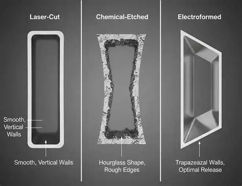
Step stencils accommodate volume disparities on mixed boards, stepping down for fine-pitch zones. IPC-7525C specifies keep-out distances: 0.9 mm per 0.025 mm step height from thin-area apertures to walls. Step-up adds thickness for large pads without compromising fine features. Fabrication methods matter - laser-cut yields trapezoidal walls for easy release, electroformed offers smoothest surfaces for ultra-fine pitch. Chemical etching suits high-volume but limits resolution.
Hybrid approaches combine techniques for cost-effectiveness. Surface treatments like nano-coatings reduce friction, boosting transfer efficiency. These optimize SMT assembly for complex, high-mix production. Troubleshooting starts with verifying step integrity to avoid gasketing failures.
Related Reading: The Complete Guide to Stencil Design for PCB Assembly
Troubleshooting Solder Paste Deposition Issues
Insufficient paste signals low area ratios or thick stencils; solutions include aperture enlargement or thinning. Bridging stems from oversized apertures or misalignment - shrink by 5-10% and check registration. Solder balls on chips resolve with home-plate designs reducing inner volume. Tombstoning indicates unequal deposits; symmetrize apertures and inspect paste rheology per J-STD-005 slump tests.
Voids arise from trapped flux; grid apertures and via alignment mitigate this. Process tweaks like squeegee pressure complement design fixes. Systematic application of SMT stencil design guidelines halves defect rates. Document changes for yield tracking.
Conclusion
Mastering solder paste stencil design unlocks perfect SMT assembly through precise control of deposition accuracy. Key elements - aspect and area ratios, thickness selection, and tailored apertures - align with IPC-7525C to minimize defects. Practical shapes and step techniques handle diverse components, while troubleshooting ensures robustness. Engineers gain confidence in scaling designs. Prioritize these SMT stencil design guidelines for reliable, high-yield production.
FAQs
Q1: What are the main SMT stencil design guidelines for solder paste deposition accuracy?
A1: SMT stencil design guidelines emphasize aspect ratios above 1.5 and area ratios over 0.66 per IPC-7525C. Aperture sizes reduce slightly from pads to contain paste, with shapes like home-plate preventing balls. Thickness matches finest pitch, verified via calculations. These ensure 75-85% transfer efficiency, reducing defects in fine-pitch assemblies. Always check the 5-ball rule for powder compatibility.
Q2: How do you select stencil thickness for optimizing SMT assembly?
A2: Stencil thickness selection bases on component pitch: around 0.125 mm for 0.5 mm pitch, thinner for below 0.4 mm. IPC-7525C tables guide choices, prioritizing fine features. Thicker stencils suit volume-heavy parts, and step stencils bridge mixed-tech needs. Balance with area ratio to maintain release, and validate with test prints for specific pastes.
Q3: What aperture size for SMT components improves deposition accuracy?
A3: Use about 1 mil reduction per side on gull-wing leads, 1:1 with radiusing for BGAs, and 1:1 for QFN perimeter pads. Cut QFN thermal pad volume by roughly 20-50% using windowpane grids. Adapt shapes (e.g., home-plate, bow-tie) to mitigate common defects, and maintain required ratios per IPC-7525C to prevent bridging while ensuring proper fillets.
Q4: Why is area ratio critical in stencil thickness selection?
A4: Area ratio above 0.66 promotes paste release regardless of thickness. Low ratios combined with thick stencils leave residue in apertures and hurt accuracy. IPC-7525C formulas account for geometry; finer powders per J-STD-005 can support lower effective ratios. Optimize iteratively with print trials to maximize yield.
References
[1] IPC-7525C — Stencil Design Guidelines. IPC, 2021. https://pcbsync.com/ipc-7525
[2] SMT Stencils 101 — What Are Industry-Standard Stencil Designs? I-Connect007, 2019.
[3] J-STD-005B — Requirements for Soldering Pastes. JEDEC/IPC, 2024. https://pcbsync.com/j-std-005


