 ALLPCB


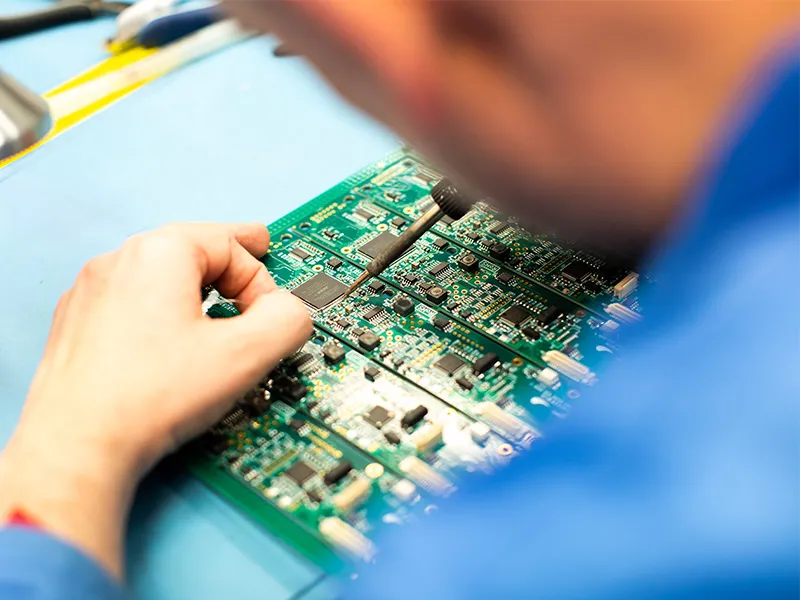
If you're looking to perfect the art of PCB assembly, understanding the selective soldering process is essential. This technique offers precision and efficiency, especially for complex boards with through-hole components. In this guide, we'll dive deep into the selective soldering process, explore the right equipment, discuss PCB design considerations, identify common defects, and provide troubleshooting tips to ensure flawless results. Whether you're an engineer or a manufacturer, this comprehensive resource will help you master selective soldering for your projects.
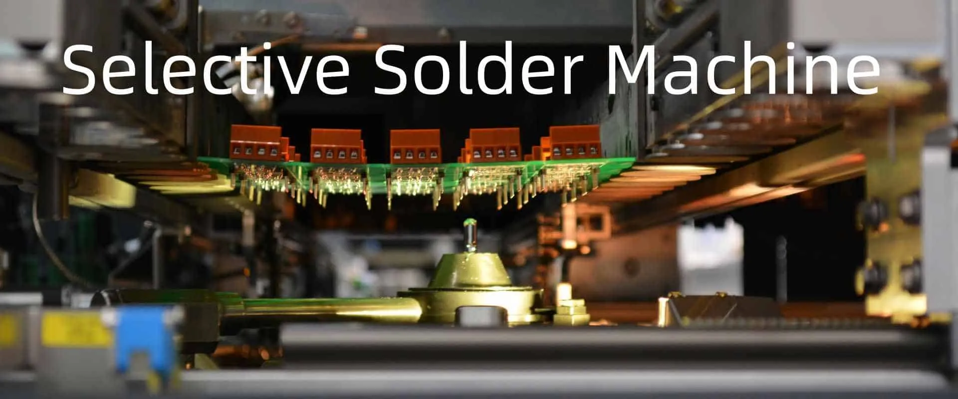
What is Selective Soldering and Why Does It Matter?
Selective soldering is a specialized technique used in PCB assembly to solder specific through-hole components on a printed circuit board (PCB). Unlike wave soldering, which solders all components in a single pass, selective soldering targets only designated areas, making it ideal for mixed-technology boards with both surface-mount and through-hole components. This precision reduces thermal stress on sensitive parts and minimizes the risk of defects.
The importance of selective soldering lies in its ability to handle modern PCB designs that often feature a mix of component types. With the rise of compact electronics, manufacturers need a process that can solder specific areas without affecting nearby components. By mastering selective soldering, you can achieve higher quality, reduce costs, and improve the reliability of your PCB assemblies.
Understanding the Selective Soldering Process
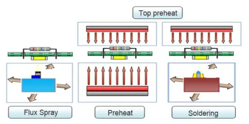
The selective soldering process involves several key steps to ensure accurate and reliable soldering. Here's a breakdown of how it works:
- Preheating: The PCB is preheated to a specific temperature, typically between 80°C and 120°C, to reduce thermal shock when the solder is applied. Preheating also activates flux, which helps clean the surfaces for better solder adhesion.
- Flux Application: Flux is applied to the targeted areas to remove oxides and ensure proper wetting of the solder. This step is crucial for achieving strong joints and preventing defects like poor wetting.
- Soldering: A precise solder nozzle or fountain moves to the designated through-hole pins, applying molten solder (often at temperatures around 260°C to 300°C) to form the joints. The nozzle's movement is controlled by software for accuracy.
- Cooling: After soldering, the PCB cools down gradually to solidify the solder joints and prevent thermal stress or cracking.
This process is highly automated, often using programmable machines to ensure consistency across large production runs. By controlling parameters like solder temperature, nozzle speed, and preheat levels, manufacturers can achieve optimal results for various board designs.
Choosing the Right Selective Soldering Equipment
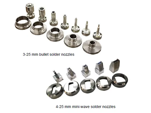
Selecting the appropriate selective soldering equipment is critical for achieving high-quality results. Here are the main factors to consider when choosing a machine for your PCB assembly needs:
- Nozzle Types: Different nozzles are available for various applications, such as mini-wave nozzles for small pins or larger nozzles for bigger components. Ensure the equipment supports interchangeable nozzles for flexibility.
- Automation Level: Fully automated systems with programmable controls offer precision and repeatability, ideal for high-volume production. Semi-automated systems may suffice for smaller runs or prototyping.
- Temperature Control: Look for equipment with precise temperature regulation (within ±1°C) to maintain consistent solder quality and prevent overheating components.
- Compatibility: Ensure the machine can handle your PCB sizes and thicknesses, as well as the specific solder alloys you plan to use, such as lead-free options.
- Maintenance and Support: Opt for equipment with accessible spare parts and reliable technical support to minimize downtime during production.
Investing in high-quality selective soldering equipment can significantly reduce defects and improve efficiency. For example, advanced systems can process up to 500 joints per hour, depending on the complexity of the board, making them a valuable asset for large-scale manufacturing.
Selective Soldering PCB Design: Best Practices
Designing a PCB with selective soldering in mind can prevent many issues during the assembly process. Here are some best practices to optimize your PCB layout for this technique:
- Component Spacing: Maintain adequate spacing between through-hole components and nearby surface-mount parts to avoid thermal interference. A minimum clearance of 2-3 mm is often recommended.
- Pad and Hole Sizes: Ensure that through-hole pads and holes are sized correctly for the components. For instance, a hole diameter of 1.2 times the lead diameter typically allows for proper solder flow.
- Thermal Relief: Use thermal relief patterns on pads connected to large ground planes to prevent heat dissipation issues during soldering. This helps achieve uniform heating and strong joints.
- Orientation: Align components in a way that allows the solder nozzle to access all targeted areas without obstruction. Avoid placing tall components in the path of the nozzle's movement.
- Flux Compatibility: Design your board to work with the type of flux used in selective soldering, ensuring that residues won't interfere with other components or testing processes.
By incorporating these design considerations, you can minimize the risk of defects and ensure a smoother selective soldering process. Always simulate the soldering path during the design phase to identify potential challenges before production.
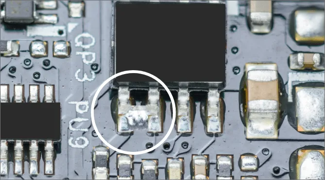
Common Selective Soldering Defects and How to Identify Them
Even with the best equipment and design practices, selective soldering defects can occur. Recognizing these issues early is key to maintaining quality. Below are some of the most common defects associated with the selective soldering process:
- Insufficient Solder: This happens when not enough solder is applied, leading to weak joints. It often results from low solder temperature (below 260°C) or inadequate flux.
- Solder Bridging: Excess solder can create unintended connections between adjacent pins, often due to improper nozzle alignment or excessive solder flow.
- Poor Wetting: If the solder doesn't adhere properly to the pad or lead, it can lead to unreliable joints. This is typically caused by contamination or insufficient flux activation.
- Thermal Damage: Overheating (above 300°C for extended periods) can damage components or the PCB itself, leading to delamination or burnt areas.
- Solder Balls: Small spheres of solder can form around the joint, often due to rapid cooling or improper flux application, posing a risk of short circuits.
Regular inspection using visual checks or automated optical systems can help detect these defects. For instance, a joint with insufficient solder might appear dull or incomplete under magnification, while bridging can be spotted as an unintended connection between pins.
Selective Soldering Troubleshooting: Tips for Flawless Results
When defects occur, effective selective soldering troubleshooting can save time and resources. Here are actionable tips to address common issues and ensure consistent quality:
- Insufficient Solder: Check the solder temperature and increase it if below the recommended range (260°C-300°C). Also, verify that the preheat temperature is sufficient (around 100°C) to prepare the board. Ensure the nozzle is clean and delivering the correct amount of solder.
- Solder Bridging: Adjust the nozzle's position and reduce the solder flow rate. Review the PCB design to ensure adequate spacing between pins (at least 2 mm). Slowing down the nozzle's movement can also prevent excess solder buildup.
- Poor Wetting: Confirm that the flux is fresh and applied evenly. Clean the PCB surface to remove any contaminants like dust or grease. If the issue persists, consider increasing the preheat time to fully activate the flux.
- Thermal Damage: Monitor the soldering temperature and duration closely. Use a machine with precise control to avoid exceeding 300°C for more than a few seconds. Incorporate thermal relief designs to manage heat distribution.
- Solder Balls: Optimize the cooling rate to prevent rapid solidification of excess solder. Ensure the flux amount is appropriate—too much can lead to spattering. Regularly clean the soldering area to remove stray solder particles.
Documenting each troubleshooting step and outcome can help identify patterns and prevent recurring issues. Additionally, performing regular maintenance on your selective soldering equipment—such as cleaning nozzles and calibrating temperature settings—can reduce the likelihood of defects.
Benefits of Mastering Selective Soldering for PCB Assembly
Mastering the selective soldering process offers numerous advantages for PCB assembly, especially in today’s fast-paced electronics industry. Here are some key benefits:
- Enhanced Precision: Selective soldering targets specific areas, reducing the risk of damage to nearby components and ensuring high-quality joints.
- Cost Efficiency: By minimizing defects and rework, this process lowers production costs. It also reduces the need for manual soldering, saving labor expenses.
- Versatility: It’s suitable for a wide range of PCB designs, including those with mixed technologies or dense component layouts.
- Improved Reliability: Properly soldered joints enhance the durability and performance of the final product, leading to fewer field failures.
For manufacturers handling high-mix, low-volume production, selective soldering provides the flexibility to adapt to varying designs without compromising quality. This adaptability can be a competitive edge in delivering reliable electronics to the market.
Conclusion: Elevate Your PCB Assembly with Selective Soldering
Selective soldering is a game-changer for PCB assembly, offering precision, efficiency, and reliability for complex board designs. By understanding the selective soldering process, investing in the right equipment, optimizing PCB layouts, and mastering troubleshooting techniques, you can significantly improve your manufacturing outcomes. Whether you're dealing with common defects or fine-tuning your setup, the tips and best practices in this guide provide a solid foundation for success.
Start implementing these strategies today to elevate the quality of your PCB assemblies. With selective soldering, you're not just assembling boards—you're building the future of electronics with unmatched accuracy and care.


