ALLPCB


Introduction
Mixed-signal printed circuit boards integrate analog and digital circuitry on the same board, creating unique challenges for power distribution. Digital sections generate high-frequency switching noise that can couple into sensitive analog paths, degrading signal quality and overall performance. Effective power distribution network design maintains low impedance paths for power delivery while isolating noise sources. Power integrity in mixed-signal design becomes critical as board densities increase and operating speeds rise. This article explores structured approaches to mixed-signal PCB power distribution, focusing on proven engineering principles. Engineers can achieve clean power delivery by prioritizing plane layouts, decoupling strategies, and noise mitigation techniques.
What Is Mixed-Signal PCB Power Distribution and Why It Matters
A power distribution network in mixed-signal PCBs delivers stable voltage to both analog and digital components while minimizing voltage droop and noise. The PDN consists of power and ground planes, vias, decoupling capacitors, and traces that form a low-impedance path from the power entry point to loads. In mixed-signal environments, digital transients from clock edges and data switching propagate through the PDN, potentially corrupting analog signals like those in ADCs or amplifiers. Poor power integrity leads to increased bit error rates, harmonic distortion, and failed compliance tests. Adhering to guidelines in IPC-2221C ensures reliable conductor sizing and spacing for power paths. Ultimately, robust PDN design directly impacts system reliability and performance margins in applications such as data acquisition and RF modules.
Fundamental Principles of Power Integrity in Mixed-Signal Design
Power integrity focuses on maintaining stable supply voltages across the frequency spectrum, from DC to high-frequency transients. The PDN impedance profile must remain low, typically targeted below milliohms up to the maximum switching frequency. Simultaneous switching noise arises when multiple digital outputs change state, causing inductive voltage drops in the PDN. Resonance peaks in the impedance curve can amplify noise if not damped properly. Ground bounce occurs when return currents overload ground paths, shifting reference potentials. Engineers model these effects using target impedance formulas derived from voltage tolerance, current draw, and capacitance.
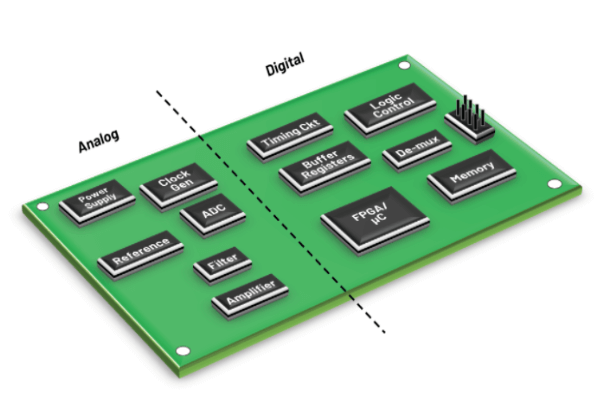
In mixed-signal boards, analog sections require quieter power than digital ones, necessitating partitioned supplies. Shared planes risk noise spillover through slot resonances or via coupling. Dedicated analog power planes, returned to isolated ground planes, preserve signal-to-noise ratios. Layer stackup influences plane coupling, adjacent power-ground pairs exhibit lower inductance. Fabricating boards per IPC-2152 guidelines verifies current-carrying capacity in planes, preventing thermal hotspots.
Power Plane Design Considerations
Power plane design forms the backbone of mixed-signal PCB power distribution by providing distributed capacitance and low resistance. Solid copper pours minimize DC resistance, while splits isolate analog and digital domains. However, splits introduce impedance discontinuities if not managed, leading to current crowding at edges. Vias stitching planes to components must align with current flow paths to avoid bottlenecks. Plane thickness, governed by copper weight, balances resistance with mechanical stability in multilayer stackups.
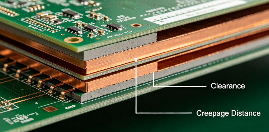
Guard traces or moats around splits prevent fringe field coupling between domains. Power plane pairs with ground planes directly above or below reduce loop inductance, enhancing high-frequency performance. In high-current designs, IPC-2152 provides data for temperature rise predictions in planes under load. Engineers simulate plane impedance using 2D field solvers to identify weak points early. Optimal splits maintain at least three times the dielectric thickness from crossing signals to avoid crosstalk.
Decoupling Capacitors for Mixed-Signal PCBs
Decoupling capacitors stabilize local supply nodes by supplying charge during transients, forming a parallel LC network with plane inductance. Place capacitors as close as possible to IC power pins, ideally within 1-2 mm, to minimize loop area. Use a range of values: bulk electrolytics for low frequencies, ceramics from 0.1 μF to 10 nF for mid-range, and smallest 1 nF for GHz bypass. Multiple parallels broaden the effective bandwidth, countering ESL and ESR limitations of singles. Via placement under capacitor pads connects directly to planes, reducing parasitic inductance.
In mixed-signal designs, analog sections need low-ESR, low-noise dielectrics like C0G, while digital tolerates X7R. Ferrite beads in series with digital supplies filter mid-frequencies without affecting DC. Board parasitics interact with caps, so stackup capacitance supplements discrete ones. Simulate PDN impedance post-placement to verify target profiles. Proper decoupling reduces power supply noise in mixed-signal circuits by over 20 dB across octaves.
Related Reading: Designing Power Distribution Networks (PDNs) for High Speed Digital Circuits
Best Practices for Reducing Power Supply Noise in Mixed-Signal Circuits
Partition the board into analog and digital zones during initial placement to localize noise. Route digital signals away from analog traces, using ground planes as shields. Separate power entry points for domains, with linear regulators or LDOs cleaning analog rails. Minimize via count in PDN paths, use blind or buried vias for dense boards. Spread high-current loads evenly to avoid localized heating.
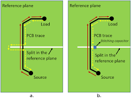
Implement stitching vias along split edges every half wavelength at peak frequencies. For multilayer boards, interleave power-ground pairs throughout the stackup. Pre-emphasis on clocks or spread-spectrum techniques soften digital edges. Verify designs with time-domain reflectometry for discontinuities. These practices ensure power integrity in mixed-signal design meets stringent noise budgets.
Related Reading: PCB Stackup Design Guidelines for Analog and Digital Circuits
Troubleshooting Common PDN Issues in Mixed-Signal PCBs
Excessive ripple often traces to insufficient bulk capacitance near regulators. Measure with spectrum analyzers probing power pins directly. Ground loops form if analog grounds tie digitally, use single-point connections at board entry. Simulate before fab to predict resonances matching observed spurs. EMI probes isolate plane radiation sources.
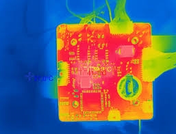
Via inductance spikes appear as high-frequency droop, add inline caps. Thermal expansion mismatches warp planes in thick copper, select CTE-matched cores. Post-assembly, scope jitter correlates to PDN noise. Iterative prototyping refines cap values. Compliance with IPC-2221C during layout catches spacing violations early.
Conclusion
Effective power distribution network design in mixed-signal PCBs demands careful integration of planes, decoupling, and partitioning. Low-impedance PDNs preserve analog fidelity amid digital aggression. Power plane design considerations like splits and stitching prevent crosstalk. Decoupling capacitors for mixed-signal PCBs provide essential local reservoirs. Reducing power supply noise in mixed-signal circuits through best practices yields robust performance. Engineers applying these principles achieve reliable, high-fidelity systems.
FAQs
Q1: What are the main challenges in mixed-signal PCB power distribution?
A1: Digital switching generates broadband noise that couples via shared PDN to analog circuits, causing distortion. Solutions include domain partitioning and dedicated planes. Proper decoupling capacitors for mixed-signal PCBs filter transients effectively. Following IPC guidelines ensures structural integrity under load.
Q2: How do decoupling capacitors improve power integrity in mixed-signal design?
A2: They shunt high-frequency currents locally, stabilizing voltage at pins and damping PDN resonances. Place arrays close to loads with varied values for broad bandwidth. This reduces power supply noise in mixed-signal circuits significantly. Simulate impedance to optimize selection.
Q3: What power plane design considerations are critical for noise isolation?
A3: Use solid pours with controlled splits, stitching vias along edges, and adjacent ground pairing. Avoid signals crossing splits perpendicularly. IPC-2152 aids in sizing for current without excess heat. These maintain low impedance across frequencies.
Q4: Why separate analog and digital grounds in mixed-signal boards?
A4: Common returns mix noise currents, shifting potentials and degrading SNR. Isolated planes with star-point tie preserve references. Ferrites or inductors further filter. This upholds power integrity in mixed-signal design reliably.
References
IPC-2221C — Generic Standard on Printed Board Design. IPC, 2023
IPC-2152 — Standard for Determining Current-Carrying Capacity in Printed Board Design. IPC, 2009