ALLPCB


In the fast-paced world of electronics, designing power distribution networks (PDNs) for high-speed digital circuits is a critical task. A well-designed PDN ensures stable power delivery, minimizes noise, and supports the performance of modern high-speed devices. Whether you're working on processors, memory modules, or communication systems, understanding PDN design, high-speed PDN challenges, and achieving a low impedance PDN is essential. In this comprehensive guide, we'll walk you through the fundamentals of PDN design, key components, analysis techniques, and actionable tips to optimize power delivery in high-speed circuits.
What Is a Power Distribution Network (PDN) and Why Does It Matter?
A Power Distribution Network (PDN) is the system of components and traces on a printed circuit board (PCB) that delivers power from the source to the various components of a circuit. In high-speed digital circuits, the PDN must supply clean, stable voltage while handling rapid current changes without introducing noise or voltage drops. A poorly designed PDN can lead to signal integrity issues, electromagnetic interference (EMI), and even system failures.
For high-speed applications, such as those operating at frequencies above 1 GHz, the PDN must maintain a low impedance across a wide range of frequencies to prevent power supply noise from affecting performance. With the right design approach, you can ensure reliable operation and meet the strict demands of modern electronics.
Key Challenges in High-Speed PDN Design
Designing a high-speed PDN comes with unique challenges due to the rapid switching speeds and high current demands of digital circuits. Here are some of the primary hurdles engineers face:
- Rapid Current Transients: High-speed circuits, such as microprocessors, can demand sudden spikes in current (up to several amperes in microseconds). The PDN must respond without causing significant voltage drops.
- Noise and EMI: Switching noise from digital components can couple into the power supply, creating interference that affects signal integrity.
- Impedance Control: Maintaining a low impedance PDN across a broad frequency spectrum (from DC to several GHz) is critical to minimize voltage fluctuations.
- Space Constraints: Modern devices are compact, leaving little room for extensive power planes or numerous decoupling capacitors.
Addressing these challenges requires a deep understanding of PDN components and careful planning during the design phase.
Core Principles of PDN Design for High-Speed Circuits
To achieve a robust PDN design for high-speed digital circuits, follow these core principles. Each focuses on minimizing noise, maintaining stability, and ensuring efficient power delivery.
1. Maintain Low Impedance Across Frequencies
A low impedance PDN is the foundation of stable power delivery. Impedance in a PDN arises from the resistance, inductance, and capacitance of traces, planes, and components. At high frequencies, inductance becomes a dominant factor, causing voltage drops during rapid current changes.
To achieve low impedance:
- Use wide power and ground planes to reduce resistance and inductance. For example, a power plane with a width of 1 inch can reduce inductance by up to 50% compared to narrow traces.
- Place decoupling capacitors close to the power pins of ICs to provide a local charge reservoir and minimize impedance at high frequencies (e.g., above 100 MHz).
- Design for minimal loop inductance by keeping power and ground paths short and direct.
2. Optimize Power and Ground Planes
Power and ground planes are critical in high-speed PDN designs. They provide a low-impedance path for current and help distribute power evenly across the board. Here’s how to optimize them:
- Place power and ground planes adjacent to each other in the PCB stack-up to create a natural capacitance (e.g., 1-2 nF per square inch with a 10-mil dielectric spacing).
- Avoid splitting planes unnecessarily, as splits can increase inductance and create noise.
- Use multiple vias to connect components to planes, reducing via inductance. For instance, using 4 vias instead of 1 can cut inductance by approximately 75%.
3. Strategic Use of Decoupling Capacitors
Decoupling capacitors are essential PDN components that supply instantaneous current to ICs during transients, reducing noise. In high-speed designs:
- Use a mix of capacitor values (e.g., 0.1 μF, 1 μF, and 10 μF) to cover a wide frequency range. Smaller capacitors handle higher frequencies (above 100 MHz), while larger ones manage lower frequencies (below 1 MHz).
- Place capacitors as close as possible to IC power pins to minimize trace inductance. A placement within 0.1 inches can reduce inductance by up to 30%.
- Consider using low-ESL (equivalent series inductance) capacitors for frequencies above 500 MHz.
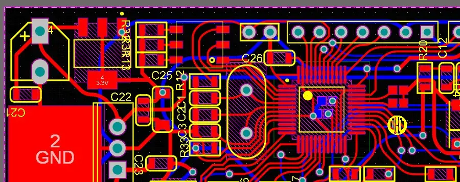
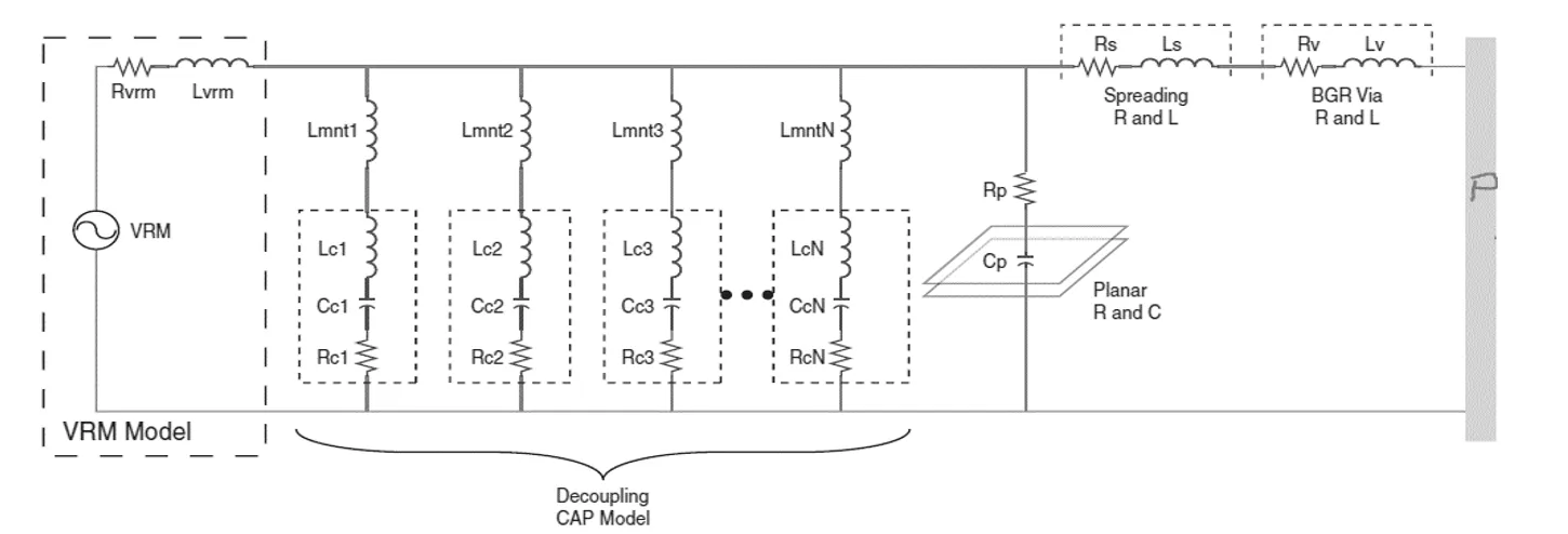
Key PDN Components for High-Speed Designs
Understanding the role of each component in a PDN is vital for effective design. Here’s a breakdown of the primary PDN components and their contributions to high-speed performance:
- Voltage Regulator Modules (VRMs): VRMs convert input voltage to the required levels for ICs (e.g., 1.2V or 3.3V). Choose VRMs with fast transient response times (under 10 μs) for high-speed applications.
- Power and Ground Planes: These provide low-impedance paths and act as a reference for signals, reducing noise.
- Decoupling Capacitors: As mentioned, they stabilize voltage by supplying current during transients.
- Ferrite Beads: These filter high-frequency noise from the power supply, often used in series with capacitors to create a low-pass filter.
PDN Analysis Techniques for High-Speed Circuits
Thorough PDN analysis ensures that your design meets performance requirements. Modern tools and techniques allow engineers to simulate and verify PDN behavior before fabrication. Here are key methods for effective analysis:
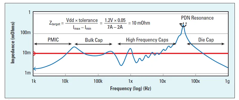
1. Target Impedance Analysis
Target impedance is the maximum allowable impedance of the PDN to keep voltage noise within acceptable limits (e.g., ±5% of nominal voltage). For a circuit drawing 10A peak current at 1.2V with a 5% tolerance, the target impedance is:
Target Impedance = (1.2V × 0.05) / 10A = 0.006 ohms (6 mΩ)
Use simulation tools to plot the PDN impedance over frequency and ensure it stays below the target. If it exceeds, add more capacitors or adjust plane design.
2. Time-Domain Simulation
Simulate transient responses to see how the PDN handles sudden current demands. For example, a 5A current step in 1 μs should not cause a voltage drop exceeding 60 mV for a 1.2V rail with 5% tolerance.
3. Frequency-Domain Analysis
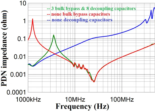
Analyze the PDN in the frequency domain to identify resonances (peaks in impedance). Resonances between 10 MHz and 100 MHz are common due to interactions between capacitors and plane inductance. Dampen these by adjusting capacitor values or adding damping resistors.
Practical Tips for Designing a Low Impedance PDN
Creating a low impedance PDN requires attention to detail during layout and component selection. Here are actionable tips to guide your design process:
- Minimize Via Inductance: Use multiple small vias (e.g., 8-10 mil diameter) for power connections instead of a single large via. This can reduce inductance from 1 nH to 0.2 nH per via path.
- Short Trace Lengths: Keep traces between capacitors and IC pins under 0.5 inches to limit parasitic inductance.
- Stack-Up Design: In a 6-layer PCB, place power and ground planes on layers 2 and 5 for tight coupling and reduced noise.
- Component Placement: Group high-current components together to minimize current loop areas and reduce EMI.
Common Mistakes to Avoid in High-Speed PDN Design
Even experienced engineers can make errors in PDN design. Avoid these common pitfalls to ensure reliability:
- Insufficient Decoupling: Using too few capacitors or placing them too far from ICs can lead to voltage drops during transients.
- Poor Plane Design: Splitting power planes or using thin traces for high-current paths increases impedance and noise.
- Ignoring High-Frequency Effects: Failing to account for frequencies above 1 GHz can result in unexpected resonances and noise.
Conclusion: Building Reliable High-Speed PDNs
Designing a power distribution network for high-speed digital circuits is a complex but rewarding process. By focusing on low impedance PDN principles, selecting the right PDN components, and conducting thorough PDN analysis, you can ensure stable power delivery and optimal performance. Whether you're tackling a high-speed PDN for a processor or a communication module, the strategies outlined in this guide will help you navigate the challenges and achieve success.
Start by planning your power and ground planes, strategically placing decoupling capacitors, and using simulation tools to validate your design. With careful attention to detail, your PDN design will support even the most demanding high-speed applications.