 ALLPCB


Insufficient solder mask clearance creates serious problems during PCB assembly. When the solder mask does not maintain proper distance from pads or traces, solder can bridge unintended areas or mask material can encroach on connection points. Engineers and assembly teams encounter these issues when design rules fall short or when manufacturing tolerances exceed expectations. The result often includes open circuits, short circuits, or weakened joints that fail under thermal or mechanical stress. Addressing clearance early in the design phase prevents costly rework and improves overall yield.
Why Solder Mask Clearance Matters in Modern PCB Assembly
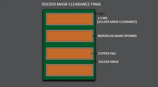
Solder mask clearance defines the minimum distance between the edge of a copper pad and the opening in the solder mask layer. This distance ensures reliable soldering while protecting adjacent conductors from unwanted solder flow. In high-density boards, even small deviations can lead to mask encroachment that blocks paste deposition or creates voids. Assembly processes become unreliable when clearance falls below recommended values, especially on fine-pitch components. Proper clearance supports consistent reflow profiles and reduces the risk of defects that appear only after thermal cycling.
Industry standards such as IPC-A-600 guide acceptable clearance limits and help teams verify board quality before assembly begins. Designers who ignore these guidelines often discover problems only after the first production run. Maintaining adequate clearance also supports long-term reliability in applications exposed to vibration or temperature extremes.
Technical Principles Behind Solder Mask Defined and Non-Solder Mask Defined Pads
Solder mask defined pads rely on the mask opening to set the final pad size, while non-solder mask defined pads allow the copper pad itself to determine the land area. In solder mask defined designs, the mask overlaps the copper edges, which can reduce the effective soldering area if clearance is insufficient. Non-solder mask defined pads provide more copper for solder attachment but require tighter control of mask positioning to avoid encroachment on traces.
Clearance calculation begins with the minimum mask opening required by the fabricator plus allowances for registration tolerances and etching variations. Typical values range from 0.05 mm to 0.15 mm depending on board thickness and copper weight, though exact figures must follow specific design rules. When clearance is too small, the mask can shift during curing or lamination and partially cover the pad. This partial coverage prevents proper solder wetting and creates high-resistance joints.
Engineers calculate clearance by subtracting the maximum mask registration tolerance from the desired opening size. They then verify the result against PCB design rules that account for both solder mask defined and non-solder mask defined configurations. Insufficient clearance often appears as mask material creeping onto the pad edge, which disrupts paste release during stencil printing.
Common Causes of Insufficient Clearance and Resulting Assembly Failures
Registration errors during solder mask application represent one frequent cause of inadequate clearance. Even small misalignments of 0.05 mm can push mask material onto pad surfaces when the original clearance was marginal. Etching undercut and mask shrinkage during thermal curing further reduce available space.
Designers sometimes overlook the cumulative effect of multiple tolerances when setting clearance values. In dense layouts, adjacent traces or vias can force tighter spacing that leaves little room for safe clearance. During reflow, insufficient clearance allows solder to wick along exposed copper or creates bridges between closely spaced pads. These defects appear as tombstoning on small components or as intermittent opens after board flexure.
Troubleshooting teams often trace these failures back to clearance values that did not account for the specific mask type or copper thickness used in production. Visual inspection under magnification reveals mask encroachment as a thin film covering part of the pad, while X-ray imaging shows voids or incomplete fillet formation.
Related Reading: The role of Solder Mask on preventing solder bridges
Practical Solutions and PCB Design Rules for Preventing Solder Mask Encroachment
Teams prevent solder mask encroachment by establishing clear minimum clearance values early in the layout process. A practical starting point is to add at least 0.075 mm to the fabricator’s stated registration tolerance for each side of the pad. Designers then review the entire board for areas where traces or vias approach pads and adjust spacing accordingly.
Using non-solder mask defined pads in high-reliability sections provides extra copper area and reduces sensitivity to mask shift. When solder mask defined pads are required for finer pitch, increasing the mask opening slightly while maintaining copper pad size helps maintain adequate clearance. Regular design rule checks that include mask-specific constraints catch problems before files reach the fabricator.
Assembly engineers verify clearance on incoming boards by measuring the distance from pad edge to mask opening with calibrated optical tools. Any board falling below the agreed minimum returns for correction rather than proceeding to paste printing. This step eliminates most downstream soldering defects related to mask issues.
Troubleshooting Steps When Clearance Problems Appear During Assembly
When solder bridges or incomplete joints appear after reflow, the first troubleshooting action is to inspect mask clearance on a sample board. Measuring several pads across different regions reveals whether encroachment is uniform or localized to certain areas. If clearance measures below specification, the lot can be reworked by selective mask removal or replaced with corrected boards.
Stencil inspection follows next, because insufficient clearance can cause paste to smear onto mask surfaces and reduce volume on the pad. Adjusting stencil aperture size or using a thinner foil sometimes compensates for minor clearance shortfalls, but this remains a temporary measure. Long-term fixes require updating the design rules and communicating new clearance targets to the layout team.
Thermal profiling during reflow also helps, because boards with marginal clearance may need slower ramp rates to allow solder to flow properly around any remaining mask edge. Documenting each defect with photographs and measurements supports root-cause analysis and prevents recurrence on future builds.
Related Reading: Understanding Solder Mask Expansion Rules in PCB DFM
Conclusion
Insufficient solder mask clearance undermines solder joint integrity and increases defect rates throughout PCB assembly. By understanding the differences between solder mask defined and non-solder mask defined pads, teams can apply targeted design rules that maintain safe spacing. Consistent verification against established guidelines, combined with practical troubleshooting, keeps production running smoothly. Early attention to clearance calculation and prevention of mask encroachment delivers reliable boards that meet performance expectations without repeated rework.
FAQs
Q1: What is the recommended approach for solder mask clearance calculation in dense PCB layouts?
A1: Engineers start by adding the fabricator’s maximum registration tolerance to both sides of each pad and then verify the result against PCB design rules. This method accounts for etching variation and mask shrinkage while supporting both solder mask defined pads and non-solder mask defined pads. The resulting clearance prevents mask encroachment and supports consistent paste release during assembly.
Q2: How do solder mask defined pads differ from non-solder mask defined pads regarding clearance requirements?
A2: Solder mask defined pads use the mask opening to control final land size, which makes them more sensitive to any reduction in clearance. Non-solder mask defined pads keep the full copper area exposed, providing more tolerance for minor mask shifts. Designers choose the appropriate type based on pitch and reliability needs while ensuring clearance remains sufficient to avoid encroachment.
Q3: What steps help prevent solder mask encroachment during high-volume production?
A3: Teams establish minimum clearance values that exceed the sum of all tolerances and perform design rule checks that include mask-specific constraints. Incoming boards undergo optical measurement of clearance before stencil printing begins. When values fall short, the lot returns for correction rather than proceeding through reflow.
Q4: How does insufficient clearance affect troubleshooting during SMT assembly?
A4: Marginal clearance often produces bridges, voids, or weak fillets that appear after reflow. Inspection teams measure pad-to-mask distance on failed boards to confirm the root cause. Adjustments to stencil apertures or reflow profiles can provide short-term relief, but permanent correction requires updated PCB design rules that enforce adequate clearance.
References
IPC-A-600K — Acceptability of Printed Boards. IPC, 2020
IPC-6012E — Qualification and Performance Specification for Rigid Printed Boards. IPC, 2017
J-STD-001G — Requirements for Soldered Electrical and Electronic Assemblies. IPC, 2017


