 ALLPCB


Copper pours serve as essential elements in printed circuit board layouts, providing low-impedance return paths, heat spreading, and mechanical stability. When these large conductive areas remain isolated or poorly connected, they can resonate at frequencies that align with operating signals or external noise sources. The resulting copper pour antenna effect converts intended ground planes into unintended radiators, elevating electromagnetic interference levels across the board. Engineers working on high-speed digital or mixed-signal designs frequently encounter degraded performance traceable to this mechanism. Proper grounding strategy EMI planning from the schematic stage onward prevents such issues from reaching fabrication.
Why the Copper Pour Antenna Effect Matters in Modern Designs
Large copper regions improve thermal dissipation and reduce voltage drops in power distribution networks. At the same time, any floating or partially connected pour introduces parasitic inductance and capacitance that can form resonant structures. These structures couple energy into adjacent traces, increasing radiated emissions and susceptibility. Signal integrity copper pour problems appear most often in boards operating above 100 MHz or in environments with strict regulatory limits. Early identification during layout review saves costly respins and maintains compliance with electromagnetic compatibility requirements.
Technical Mechanisms Behind Unintended Antenna Behavior
A copper pour becomes an effective antenna when its physical dimensions approach a quarter-wavelength or half-wavelength of a signal harmonic or external field. Current flowing along the edges of the pour creates magnetic fields that radiate outward, while voltage gradients across the pour surface generate electric fields. Without sufficient low-inductance paths to the reference plane, these fields propagate rather than cancel. Parasitic coupling between the pour and nearby signal lines further amplifies the effect, turning a supposed shield into an amplifier of noise.
Grounding strategy EMI practices address this by ensuring every pour segment maintains multiple connections to the primary return plane. The number and placement of these connections determine the effective inductance seen by high-frequency currents. When connection density falls below a threshold dictated by the highest frequency of interest, the pour begins to behave as a slot or patch antenna. Temperature variations during operation can also shift resonance points slightly, making marginal designs fail in the field even if they pass initial testing.
Related Reading: PCB Copper Pour: The Ultimate Guide to Improving Your Designs
Best Practices for EMI Reduction Copper Pour Implementation
Begin by defining clear keep-out zones around high-speed differential pairs and clock lines so that pours do not encroach within three times the trace width. Divide large pours into smaller sections separated by ground traces or vias to raise the resonant frequency above the band of interest. Place stitching vias on a grid no larger than one-twentieth of the wavelength at the highest frequency, ensuring each via carries return current with minimal loop area.
Thermal relief patterns around component pads should use spoke widths sufficient to carry the required current while still providing adequate high-frequency connectivity. In regions where pours must remain solid for power integrity, add a perimeter of vias tied directly to the reference plane at intervals determined by the board stack-up. Simulation of the full layout at the target frequencies reveals current density concentrations that indicate potential antenna behavior before prototypes are built.
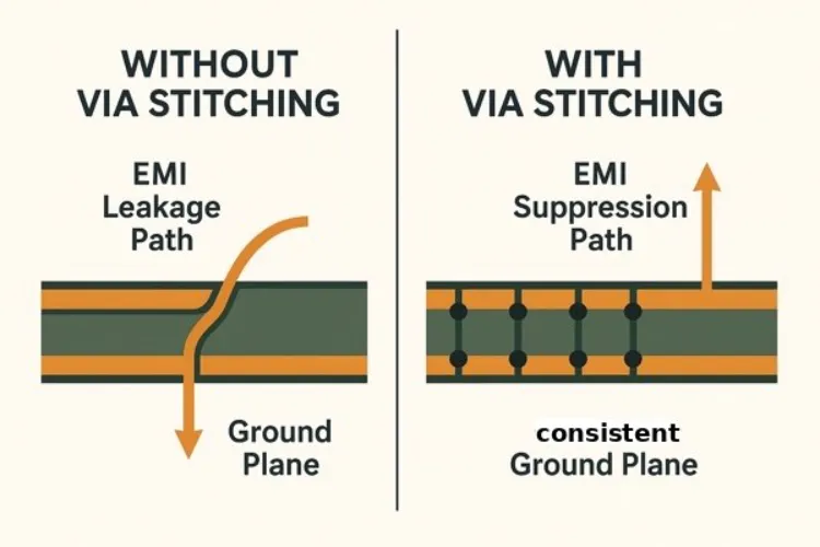
Review the stack-up early to confirm that pours on adjacent layers maintain consistent reference distances. Misaligned pours on opposite sides of a core can create parallel-plate structures that resonate independently. Consistent use of the same reference net for all pours eliminates floating islands that otherwise act as secondary antennas. Documentation of via counts and locations in the design review package supports traceability and future modifications.
Related Reading: Copper Pour for Beginners: A Simple Explanation of PCB Grounding
Practical Troubleshooting Steps During Layout and Verification
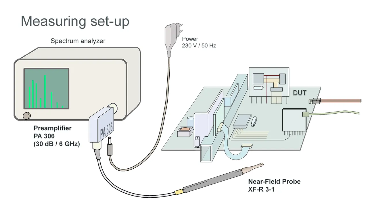
Start verification by extracting the return current paths for every net above 50 MHz using field solvers or post-layout analysis tools. Any pour segment showing current loops larger than 1 mm in diameter warrants additional vias or segmentation. Measure radiated emissions on an initial prototype using a near-field probe to locate hot spots directly above large pours. Compare results before and after adding stitching vias to quantify improvement in the copper pour antenna effect.
Adjust pour boundaries iteratively, keeping at least 0.5 mm clearance from critical signals while maintaining solid connectivity to the reference plane. Re-run signal integrity simulations after each change to confirm that eye diagrams and timing margins remain within specification. Record all modifications in the design history file so that subsequent revisions preserve the grounding strategy EMI improvements.
Conclusion
Copper pours remain valuable for thermal and power integrity when their antenna characteristics receive explicit attention during layout. Systematic application of stitching vias, segmentation, and reference plane connectivity eliminates the copper pour antenna effect without sacrificing other performance goals. Engineers who integrate these checks into standard review processes achieve both lower EMI and higher first-pass success rates. Consistent adherence to established design rules ensures repeatable results across multiple projects and fabrication cycles.
FAQs
Q1: How does the copper pour antenna effect impact signal integrity copper pour performance?
A1: Large copper areas that lack sufficient low-inductance connections to the reference plane can resonate at operating frequencies, coupling noise into nearby traces and degrading timing margins. The effect becomes measurable when pour dimensions support standing waves within the signal bandwidth. Adding stitching vias at appropriate intervals restores the intended shielding behavior while preserving thermal benefits.
Q2: What grounding strategy EMI techniques prevent copper pour antenna effects in RF designs?
A2: Multiple vias placed on a wavelength-based grid tie each pour segment directly to the primary return plane, minimizing loop inductance. Segmenting oversized pours with ground traces raises resonant frequencies above the band of interest. Consistent reference net assignment across all layers eliminates floating regions that otherwise radiate.
Q3: Why do copper pour RF design practices require specific via spacing rules?
A3: Via spacing determines the highest frequency at which the pour continues to act as a continuous low-impedance surface rather than a resonant structure. Spacing exceeding one-twentieth of the wavelength allows current concentrations that radiate energy. Following this guideline during layout review ensures the pour functions as intended across the full operating spectrum.
Q4: Can improper copper pour implementation increase overall EMI levels even in non-RF boards?
A4: Yes, digital switching harmonics can excite pours at frequencies well above the fundamental clock rate, creating broadband emissions. Without adequate grounding, these emissions couple through cables or enclosures and violate regulatory limits. Early incorporation of stitching and segmentation during layout prevents such issues from appearing during compliance testing.
References
IPC-2221B — Generic Standard on Printed Board Design. IPC, 2012
IPC-6012E — Qualification and Performance Specification for Rigid Printed Boards. IPC, 2017


