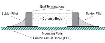
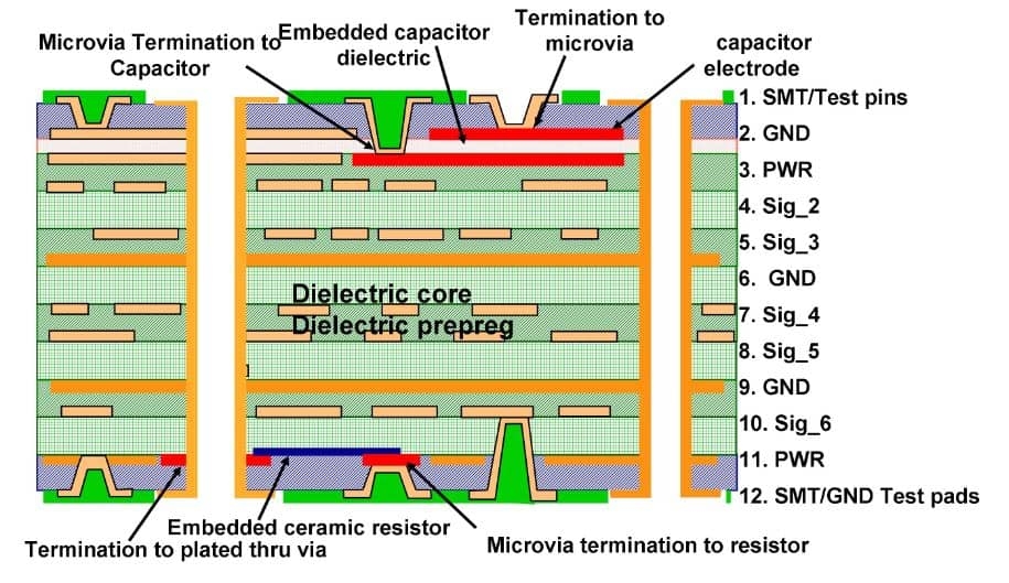
In the world of printed circuit board (PCB) design and manufacturing, solder bridges are a common defect that can lead to short circuits and malfunctioning electronics. These unwanted connections between adjacent pads or traces can be a nightmare for engineers. So, how can you prevent solder bridges and ensure a reliable PCB? The answer lies in the critical role of the solder mask. This protective layer not only shields copper traces but also acts as a barrier to stop solder from flowing where it shouldn’t. In this blog, we’ll dive deep into the importance of solder mask in preventing solder bridges, explore common PCB defects, and highlight design mistakes to avoid for a flawless board.
What Are Solder Bridges and Why Are They a Problem?
Solder bridges occur when excess solder creates an unintended connection between two or more conductive elements on a PCB, such as pads or traces. This defect often happens during the soldering process, especially in surface mount technology (SMT) assembly, where components are placed close together. The result? Electrical shorts that can cause a circuit to fail, leading to costly rework or even complete product failure.
The impact of solder bridges is significant. For instance, in high-density PCB designs, where components are packed tightly with pitches as small as 0.5 mm, the risk of bridging increases. A single short circuit can disrupt signal integrity, cause overheating, or render an entire board unusable. Preventing these defects is essential for maintaining reliability and performance in electronic devices.
Understanding the Solder Mask: A Protective Barrier
The solder mask is a thin polymer layer applied to the surface of a PCB. Its primary job is to insulate and protect the copper traces from environmental factors like moisture and dust. However, one of its most vital functions is preventing solder from adhering to areas where it’s not supposed to during the assembly process. By covering non-soldering areas, the solder mask ensures that solder only sticks to designated pads and vias.
Typically, solder mask comes in colors like green, blue, or red, with green being the most common due to its visibility and contrast during inspection. The layer is applied using a silkscreen or photo-imaging process and is usually between 0.8 to 1.2 mils (20 to 30 micrometers) thick. This thin yet robust coating plays a massive role in reducing PCB defects like solder bridges.
How Solder Mask Prevents Solder Bridges
The solder mask acts as a physical barrier that blocks solder from flowing beyond the intended areas. Here’s how it works to prevent solder bridges:
- Isolating Adjacent Pads: In designs with fine-pitch components, pads are often spaced less than 0.25 mm apart. Without a solder mask, solder can easily bridge these tiny gaps during reflow. The mask creates a defined boundary, ensuring solder stays on the pad.
- Reducing Solder Flow: During the soldering process, molten solder can spread across exposed copper. The solder mask limits this flow by covering non-essential areas, reducing the chance of accidental connections.
- Improving Assembly Precision: By clearly marking where solder should go, the mask helps align stencils during SMT assembly. This precision minimizes excess solder application, a common cause of bridges.
Common PCB Defects Related to Solder Bridges
While solder bridges are a specific defect, they often stem from broader issues in PCB design and manufacturing. Understanding these related defects can help engineers address root causes:
- Excess Solder Deposition: If too much solder paste is applied during assembly, it can overflow and connect adjacent pads. This often happens when stencil apertures are not optimized for the pad size.
- Poor Pad Spacing: In high-density designs, pads placed too close together (less than 0.2 mm apart in some cases) increase the risk of bridging, even with a solder mask.
- Solder Mask Damage or Misalignment: If the solder mask layer is scratched, misaligned, or improperly applied, it may fail to cover critical areas, exposing copper and inviting solder bridges.
By addressing these issues, you can significantly lower the chances of defects. The solder mask is a key player, but it must be applied correctly to be effective.
PCB Design Mistakes That Lead to Solder Bridges
Design errors are often the starting point for solder bridge issues. Here are some common PCB design mistakes and how they contribute to defects:
- Inadequate Solder Mask Clearance: If the solder mask opening around pads is too large, it exposes more copper than necessary, increasing the risk of solder spreading. A typical clearance should be around 0.05 mm to 0.1 mm beyond the pad edge, depending on the manufacturer’s capabilities.
- Insufficient Spacing Between Pads: Designing pads too close together, especially for fine-pitch components, leaves little room for error. Following IPC standards, such as IPC-7351, can help ensure proper spacing (e.g., a minimum of 0.25 mm for 0.5 mm pitch components).
- Ignoring Solder Mask Bridge Feasibility: For very tight spacing, some designs require a “solder mask bridge”—a small strip of mask material between pads to prevent bridging. If the spacing is below the manufacturer’s minimum bridge width (often 0.1 mm), the mask may not hold, leading to defects.
By paying attention to these design considerations, you can avoid common pitfalls that lead to solder bridges and other PCB defects.
Best Practices for Solder Mask Application to Avoid Defects
To maximize the effectiveness of the solder mask in preventing solder bridges, follow these best practices during design and manufacturing:
- Optimize Solder Mask Design: Ensure the mask openings are slightly larger than the pads (by about 0.05 mm per side) to account for manufacturing tolerances. This prevents misalignment while still protecting adjacent areas.
- Use High-Quality Materials: Choose a solder mask material with good adhesion and thermal resistance. Poor-quality masks can crack or peel during reflow, exposing copper and leading to bridges.
- Verify Manufacturer Capabilities: Different manufacturers have varying minimum solder mask bridge widths and alignment accuracies. Confirm these specs (e.g., minimum bridge width of 0.1 mm) before finalizing your design.
- Inspect for Defects: After applying the solder mask, inspect the PCB for pinholes, scratches, or incomplete coverage. Even small flaws can compromise the mask’s ability to prevent bridges.
Implementing these steps can make a huge difference in the quality and reliability of your boards.
The Role of Solder Mask in High-Density PCB Designs
In modern electronics, high-density interconnect (HDI) PCBs are increasingly common, with trace widths as narrow as 0.1 mm and pad pitches below 0.4 mm. In such designs, the risk of solder bridges skyrockets due to the tight spacing. The solder mask becomes even more critical in these scenarios.
For HDI boards, engineers often use advanced solder mask materials with higher precision application techniques, such as liquid photoimageable (LPI) masks. These materials allow for finer control, ensuring that even tiny gaps between pads are protected. Additionally, some designs incorporate “no-bridge” areas where the mask is omitted between very close pads, paired with precise stencil designs to control solder paste volume (e.g., reducing paste volume by 10-20% for fine-pitch components).
How Solder Mask Improves Overall PCB Reliability
Beyond preventing solder bridges, the solder mask contributes to the long-term reliability of a PCB in several ways:
- Protection Against Corrosion: By covering copper traces, the mask shields them from oxidation and environmental damage, which can weaken connections over time.
- Enhanced Insulation: The mask provides electrical insulation, reducing the risk of shorts caused by dust, moisture, or accidental contact.
- Better Assembly Yields: With fewer defects like solder bridges, production yields improve, saving time and cost during manufacturing.
A well-designed and properly applied solder mask is a cornerstone of a robust PCB, ensuring both immediate functionality and long-term durability.
Conclusion: Prioritizing Solder Mask for Flawless PCBs
The solder mask is more than just a protective coating—it’s a vital tool in preventing solder bridges, one of the most common PCB defects. By acting as a barrier, it stops solder from creating unwanted connections, especially in high-density designs where spacing is tight. However, its effectiveness depends on proper design practices, such as adequate clearance, correct pad spacing, and attention to manufacturing capabilities.
For engineers and designers, understanding the role of solder mask and avoiding common PCB design mistakes can mean the difference between a reliable board and a failed product. By following best practices and leveraging the protective power of the solder mask, you can minimize defects, improve assembly yields, and ensure your PCBs perform as intended. Whether you’re working on a simple prototype or a complex HDI board, never underestimate the importance of this thin yet mighty layer.
 ALLPCB


