 ALLPCB


Introduction
Pad lifting remains one of the more persistent defects encountered during surface-mount technology assembly. It occurs when a copper land separates from the underlying laminate, often after the reflow soldering stage. Engineers working on high-density boards see this issue most frequently on fine-pitch components and ball-grid arrays. The problem disrupts electrical continuity, reduces mechanical strength, and can lead to field failures if undetected. Understanding the root causes and applying disciplined process controls helps teams maintain acceptable yield levels without resorting to costly rework.
What Is Pad Lifting and Why It Matters
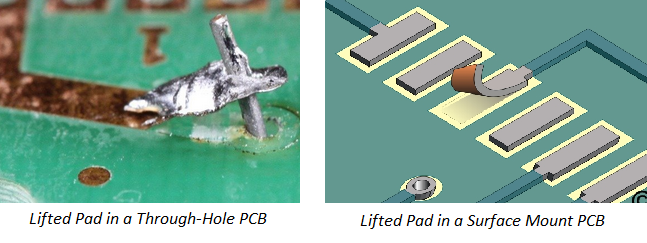
Pad lifting describes the partial or complete detachment of a copper pad from the printed-circuit-board substrate. In SMT assembly the phenomenon usually appears after the solder paste has melted and cooled. The lifted pad may remain attached to the component lead or ball, creating an open circuit or intermittent connection.
Industry experience shows that even a single lifted pad on a critical net can scrap an entire assembly. For procurement and quality teams the defect also increases inspection time and drives up scrap rates. Because modern boards use thinner laminates and higher copper densities, the mechanical margin between pad and substrate has narrowed. Addressing pad lifting early in the design and process-development cycle therefore protects both schedule and cost targets.
Technical Principles and Mechanisms
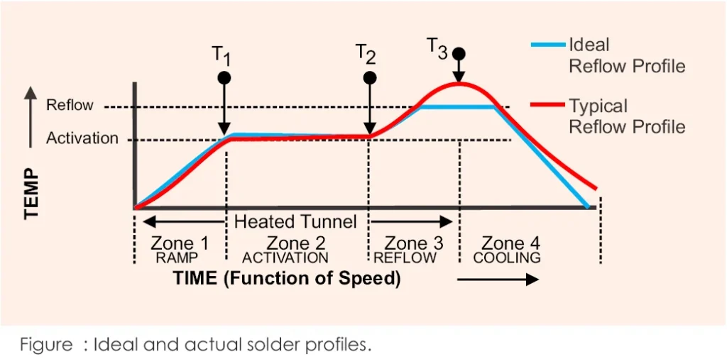
During reflow the PCB and its components experience rapid temperature changes. Copper expands and contracts at a different rate than the glass-epoxy laminate, generating shear stress at the pad-to-substrate interface. When the adhesive bond between copper and dielectric is marginal, this stress exceeds the peel strength and the pad lifts.
Solder-paste volume and reflow profile also play direct roles. Excessive paste can create a larger solder fillet that pulls harder on the pad during cooling. Conversely, insufficient paste leaves the joint weak, allowing mechanical handling to finish the separation. Component placement force and stencil release characteristics further influence the initial alignment and subsequent stress distribution.
Thermal warpage of the board or package adds another variable. As the assembly cools, any out-of-plane deformation concentrates stress on individual pads, especially those located near the corners of large components. Engineers therefore monitor both material selection and process parameters to keep cumulative stress below the threshold that initiates lifting.
Related Reading: The Ultimate Guide to PCB Pad Lifting: From Causes to Cures
Practical Solutions and Best Practices
Design teams reduce the risk of pad lifting by specifying laminates with higher glass-transition temperatures and improved copper-to-resin adhesion. Increasing the annular ring around vias and using tear-drop pad shapes distributes stress more evenly.
On the process side, reflow profiles should be tuned to minimize the time above liquidus while still achieving full solder coalescence. Reducing peak temperature by 5–10 °C often lowers the thermal gradient enough to stay within safe stress limits. Solder-paste volume is controlled through stencil aperture design and regular paste-height measurements.
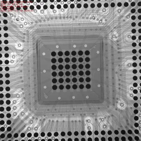
After placement, gentle handling and fixturing prevent mechanical shock that could dislodge marginally bonded pads. In-line automated optical inspection and X-ray systems catch lifted pads before they reach functional test. When a defect is found, root-cause analysis typically examines laminate lot data, stencil condition, and reflow oven calibration records.
Following established industry standards such as IPC-A-610 helps define acceptable limits for pad integrity after assembly. Process audits against J-STD-001 further ensure that soldering parameters remain within validated windows.
Troubleshooting Insights from Assembly Lines
When pad lifting appears on a new product, the first step is to isolate whether the issue is design-related or process-related. Cross-sectioning a few suspect joints quickly reveals whether the copper-to-laminate bond failed or whether excessive solder fillet volume was the culprit.
If the laminate peel strength is marginal, switching to a higher-performance material grade usually resolves the problem on subsequent builds. When the root cause traces to the reflow profile, incremental adjustments to the cooling rate often restore acceptable results without changing the bill of materials. Documenting each trial in a structured engineering change record allows the team to correlate process changes with defect rates and to maintain traceability for future audits.
Related Reading: Pad Lifting Prevention: A Proactive Approach to PCB Reliability
Conclusion
Pad lifting in SMT assembly arises from the interaction of thermal expansion mismatch, solder-joint geometry, and laminate adhesion. By combining careful material selection, controlled reflow parameters, and rigorous inspection, engineering teams can keep the defect rate low. Consistent application of recognized industry standards provides a common language for defining acceptable quality and for driving continuous improvement across design and manufacturing groups.
FAQs
Q1: What causes SMT pad lifting during reflow soldering?
A1: Pad lifting occurs when thermal expansion differences between copper and the PCB laminate exceed the adhesive strength at the pad interface. Excessive solder volume, aggressive reflow profiles, and board warpage concentrate stress on individual lands. Proper laminate selection and profile optimization reduce the likelihood of separation.
Q2: How can component placement contribute to pad lifting?
A2: High placement force or misalignment can press a component lead or ball against a pad that already has marginal adhesion. Subsequent reflow then amplifies the stress, completing the lift. Verifying placement accuracy and using appropriate nozzle pressure settings helps prevent this secondary cause.
Q3: What inspection methods detect BGA pad lifting effectively?
A3: Automated X-ray inspection reveals lifted pads beneath BGAs by showing gaps or tilted balls. Cross-sectioning provides definitive confirmation when optical methods are inconclusive. Combining both techniques gives high confidence that no lifted pads reach the customer.
Q4: Which industry standards address solder paste and pad integrity in SMT?
A4: Standards such as IPC-A-610 define visual and dimensional acceptance criteria for assembled boards, while J-STD-001 specifies soldering process requirements. Adhering to these documents helps teams establish consistent limits for pad attachment strength and joint quality.


