 ALLPCB


Introduction
In high-density PCB assembly, achieving reliable solder joints for components with pitches below 0.5 mm presents significant challenges. Fine-pitch SMT stencils serve as the cornerstone for precise solder paste deposition, directly influencing assembly yields and defect rates. As electronic devices shrink to support applications like wearables and 5G modules, engineers must prioritize stencil design to handle ultra-small apertures without compromising paste transfer. Poor stencil performance often leads to issues such as insufficient solder volume or bridging, which can cascade into reflow failures. This article explores fine pitch SMT stencil design principles, focusing on practical strategies for electric engineers tackling dense boards. By mastering these elements, teams can enhance precision and troubleshoot effectively in production environments.
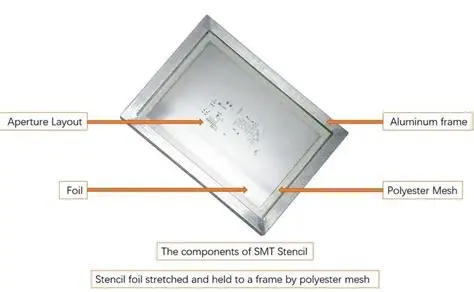
What Are Fine-Pitch SMT Stencils and Why They Matter
Fine-pitch SMT stencils feature apertures sized for component leads or pads spaced at 0.5 mm or less, enabling accurate solder paste printing on high-density boards. These stencils, typically laser-cut from stainless steel or nickel foil, transfer paste volumes as small as a few picoliters per pad. In contrast to standard stencils for coarser pitches, fine-pitch versions demand tighter tolerances to prevent defects amid shrinking component footprints. Industry trends toward miniaturization amplify their importance, as seen in assemblies packing thousands of passives like 0402 and 0201 chips. Engineers rely on them to balance paste deposition with release properties, ensuring joints meet reliability standards. Without optimized fine pitch SMT stencil design, assembly lines face higher rework costs and yield losses.
The relevance extends to troubleshooting real-world scenarios, where stencil inaccuracies amplify during high-volume runs. For instance, inconsistent aperture walls can trap paste, leading to uneven prints across panels. Adhering to guidelines like those in IPC-7525 helps mitigate these risks by standardizing parameters. Ultimately, fine-pitch stencils bridge design intent and manufacturability, making them indispensable for electric engineers pushing density limits.
Core Technical Principles of Fine Pitch SMT Stencil Design
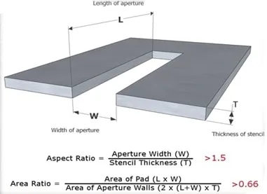
Fine pitch SMT stencil design hinges on geometric ratios that govern solder paste release and volume control. The area ratio, defined as aperture area divided by the product of perimeter and stencil thickness, must exceed 0.66 for reliable transfer, as insufficient ratios cause paste to cling to walls. Aspect ratio, the smallest aperture dimension divided by thickness, should stay above 1.0 to avoid bridging during printing. These metrics become critical below 0.4 mm pitch, where thicker foils exacerbate defects. Engineers calculate them early using pad geometries from land pattern standards to predict performance.
Stencil thickness profoundly impacts these ratios in fine-pitch applications. Thinner foils, around 0.075 to 0.125 mm, maintain favorable proportions for small apertures, promoting clean snap-off. However, excessive thinning risks mechanical fragility during printing cycles. Aperture shapes also matter: rounded rectangles outperform squares by reducing paste shear stress. IPC-7525 outlines these principles, emphasizing empirical validation through SPI data. Mastering them allows engineers to simulate print outcomes before fabrication.
Paste rheology interacts with stencil geometry, influencing transfer efficiency under squeegee pressure. Type 4 or finer pastes suit fine pitches, minimizing viscosity issues in narrow walls. Surface tension effects dominate at micro-scales, where bridging initiates if apertures are too close. Engineers troubleshoot by adjusting print speed and separation to optimize flow.
Related Reading: PCB Stencil Design for Panelization: Achieving Optimal Solder Paste Deposition
Optimizing Aperture Size for Fine Pitch and Stencil Thickness Selection
Aperture size for fine pitch directly derives from pad dimensions, typically cropped 10-25% to control volume while ensuring coverage. For pitches around 0.4 mm, widths narrow to 0.15-0.25 mm, demanding sub-micron laser accuracy. Overly large openings lead to excess paste slumping, while undersized ones starve joints. Engineers cross-reference land patterns to set baselines, then refine via DOE for specific alloys.
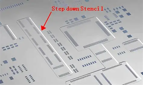
Stencil thickness for fine pitch scales inversely with aperture dimensions to preserve ratios. Foils of 0.1 mm suit most 0.3-0.5 mm pitches, dropping to 0.075 mm for ultra-fine. Step-down stencils blend thicknesses, using thinner zones for dense areas. This approach, detailed in IPC-7525, prevents global compromises. Validation involves printing trials to measure deposit height uniformity.
Home plating or electropolishing smooths walls, enhancing release without altering thickness. Engineers select based on cycle life needs, balancing cost and performance.
Best Practices for 0402 Stencil Design and 0201 Stencil Design
0402 stencil design targets components measuring 1.0 x 0.5 mm, where apertures often span 0.35-0.45 mm length by 0.25-0.35 mm width at 0.1-0.125 mm thickness. Crop pads by 15-20% lengthwise for volume equity, elongating slightly if needed. This setup yields area ratios above 0.7, minimizing tombstoning risks. Print with low-angle squeegees to shear paste evenly.
For 0201 stencil design, even tighter control applies to 0.6 x 0.3 mm chips, using 0.075-0.1 mm foils and apertures around 0.2-0.3 mm. Ultra-thin walls require nano-coatings for durability. Test prints confirm 75-85% transfer efficiency.
Both demand fiducial alignment precision under 25 μm to avoid offsets.
Related Reading: Precision Solder Paste Application: Mastering Laser Cut Stencils for Fine-Pitch PCBs
Solder Bridging Prevention in Fine-Pitch Assemblies
Solder bridging prevention starts with aperture spacing exceeding 0.15 mm between adjacent features, coupled with optimal thickness. Thinner stencils reduce paste height, limiting flow between pads during reflow. IPC J-STD-001 criteria guide joint acceptance, flagging bridges over 25% pad width.
Print parameters play a key role: snap-off distances of 1-1.5 mm and speeds below 50 mm/s curb slumping. Paste choice favors low-residue types with fine metal content. Post-print inspection via SPI flags early risks.
Troubleshooting involves aperture audits; burrs or hooks trap paste, necessitating repolishing. Panel warpage exacerbates bridging, so flatness checks precede printing.
Multi-pass printing for mixed densities aids prevention without stencil changes.
Troubleshooting Common Fine-Pitch Printing Defects
Insufficient paste volume signals poor area ratios; recalculate and thin the stencil if below 0.66. Bridging clusters near dense arrays point to excessive thickness or high pressure, addressed by DOE adjustments. Scooping occurs from fast snaps, resolved by slowing to 20-30 mm/s.
Uneven deposits across boards indicate warped stencils or boards; use vacuum support. For 0201 skips, verify paste age and humidity control. Log SPI data to correlate defects with parameters, iterating designs iteratively.
Conclusion
Fine pitch SMT stencil design demands a holistic approach integrating ratios, thickness, and process controls for high-density success. Prioritizing aperture size for fine pitch and stencil thickness for fine pitch ensures robust paste transfer, while solder bridging prevention strategies safeguard yields. Tailored 0402 and 0201 stencil designs exemplify practical application. Electric engineers benefit from standards like IPC-7525 to guide decisions. Implementing these insights reduces defects, streamlining troubleshooting and boosting assembly reliability.
FAQs
Q1: What is the ideal stencil thickness for fine pitch components like 0402?
A1: Stencil thickness for fine pitch around 0.1-0.125 mm balances ratios for 0402 designs, achieving area ratios over 0.66. Thinner foils prevent bridging but require robust handling. Validate with print trials per IPC-7525 guidelines to match specific pad crops and paste types, ensuring consistent volume across dense arrays.
Q2: How do you determine aperture size for fine pitch SMT stencil design?
A2: Aperture size for fine pitch derives from pad dimensions minus 10-25% crop, targeting widths of 0.15-0.25 mm for 0.3-0.5 mm pitches. Maintain aspect ratios above 1.0 and area ratios ≥0.66. Use land pattern data to elongate if needed for equity, troubleshooting via SPI for optimal transfer in high-density layouts.
Q3: What strategies prevent solder bridging in fine pitch assembly?
A3: Solder bridging prevention relies on thinner stencils, aperture spacing >0.15 mm, and controlled print speeds under 50 mm/s. Optimize squeegee pressure and snap-off to minimize slumping. For fine pitch SMT stencil design, electropolish walls and monitor ratios, resolving persistent issues through process DOE and defect mapping.
Q4: Why is area ratio critical in 0201 stencil design?
A4: In 0201 stencil design, area ratio ≥0.66 ensures paste release from ultra-small apertures at 0.075-0.1 mm thickness. Low ratios trap paste, causing skips or starvation. Engineers calculate it upfront, adjusting crops to hit targets and prevent bridging in dense passives.
References
IPC-7525B — Stencil Design Guidelines. IPC, 2011
IPC J-STD-001H — Requirements for Soldered Electrical and Electronic Assemblies. IPC, 2018
IPC-7351D — Generic Requirements for Surface Mount Design and Land Pattern Standard. IPC, 2014


