 ALLPCB


Introduction
In modern PCB assembly, achieving precise solder paste deposition is critical for reliable joints, especially on boards with diverse component types. Multilevel solder paste stencils address this challenge by allowing varying paste volumes in a single print operation. Electric engineers often encounter issues with mixed-technology boards where fine-pitch devices coexist with larger components requiring more solder. These stencils enable optimized paste transfer, reducing defects like bridging or insufficient solder. As assembly lines push toward higher densities, understanding multilevel stencils becomes essential for troubleshooting and process control. This article explores their principles, design, and practical use.
What Are Multilevel Solder Paste Stencils and Why Do They Matter?
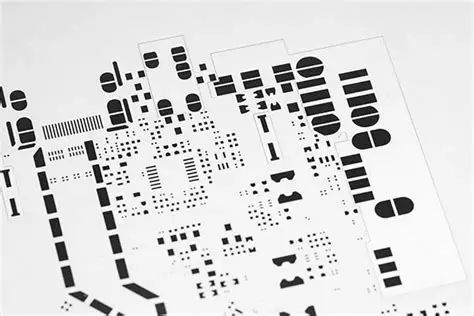
Multilevel solder paste stencils, also known as step stencils, feature apertures with different thicknesses across the same foil. Unlike traditional single-level stencils that apply uniform paste height, multilevel designs tailor paste volume to specific pads. For instance, larger components like QFNs need thicker paste deposits for robust joints, while 01005 chips require thinner layers to prevent excess buildup. This precision minimizes reflow defects and improves first-pass yields in surface mount technology processes. Electric engineers value them for high-mix production where changing stencils disrupts throughput. In essence, they bridge the gap between conflicting paste requirements on complex boards.
The relevance grows with shrinking component sizes and denser layouts. Boards mixing BGAs, connectors, and micro-resistors demand adaptive stenciling to maintain solder joint integrity. Without multilevel stencils, engineers resort to multiple prints or manual adjustments, increasing cycle time and error risk. These stencils streamline operations, aligning with demands for automation and reliability in electronics manufacturing. Their adoption directly impacts assembly efficiency and long-term board performance.
Technical Principles of Multilevel Stencils and Stencil Welding
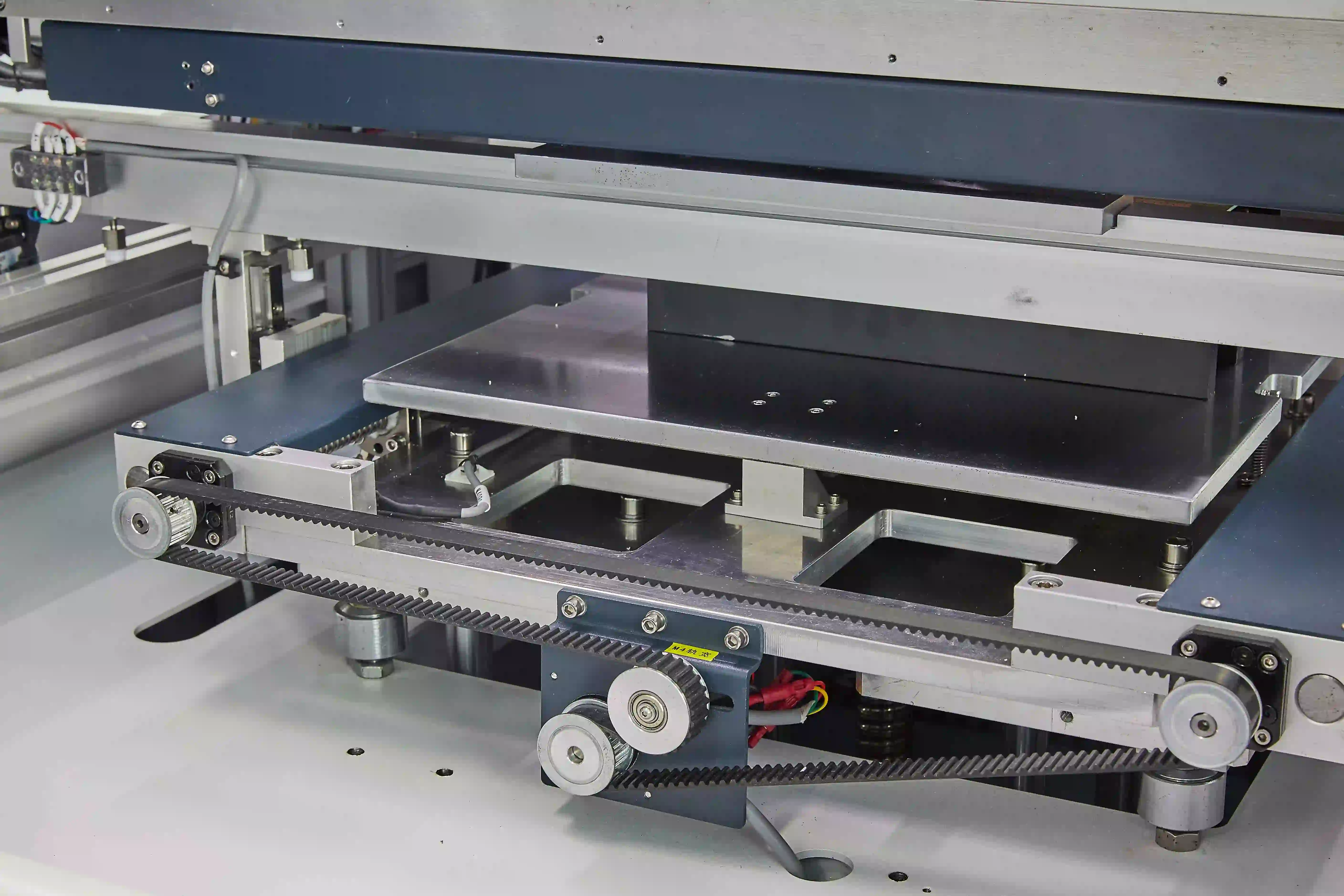
Multilevel stencils operate on the principle of controlled aperture depth to regulate solder paste release. Paste volume is proportional to aperture area times depth, so varying depths achieve targeted deposits. Engineers design steps to match land patterns, ensuring paste height matches component needs post-print. The stencil aligns precisely over the PCB, and squeegee pressure forces paste through apertures without smearing. Key to success is maintaining step integrity during printing to avoid gasketing failures between levels.
Stencil welding plays a pivotal role in constructing robust multilevel stencils from multiple foil layers. This process uses laser energy to fuse thin stainless steel or nickel foils, creating seamless transitions between thicknesses. Welding ensures structural stability under repeated printing cycles, preventing delamination or flexing. Precise control of weld parameters avoids heat-affected zones that could distort apertures. Electric engineers troubleshoot weld quality by inspecting for uniform fusion and minimal distortion post-fabrication. This technique enables complex geometries unattainable with single-foil etching alone.
Material selection influences performance, with stainless steel offering durability and nickel providing finer features. Foil thicknesses typically range from base levels suited to fine-pitch needs, stepped up for power devices. Surface treatments enhance release properties, reducing paste adhesion. Understanding these principles helps engineers predict print behavior and iterate designs effectively.
Manufacturing Processes for Multilevel Stencils
Fabrication begins with data preparation from Gerber files, defining aperture locations and step heights. Laser cutting excels for multilevel stencils due to its precision in creating tapered walls and steps. Chemical etching forms step-up or step-down features on single foils, while additive methods build layers. For advanced designs, stencil welding assembles multi-foil stacks, bonding them atomically without fillers. Post-processing includes electropolishing for smooth walls and tensioning into frames.
Quality checks verify aperture dimensions, step heights, and weld strength before deployment. Manufacturers stress-test stencils for cycle life, ensuring they withstand thousands of prints. Electric engineers collaborate early to refine designs, avoiding manufacturability issues like undercut steps. Process variations like nano-coating apertures further tune paste transfer efficiency. Overall, these methods deliver stencils ready for high-volume SMT lines.
Related Reading: Mastering Step Up Stencils: A Comprehensive Guide for PCB Assembly
Design Best Practices for Multilevel Stencils
Effective design follows guidelines like those in IPC-7525, emphasizing aspect ratios and area ratios for clean release. Aperture width should exceed 1.5 times thickness to promote gamma wipe and prevent bridging. For multilevel features, transitions must be gradual to avoid paste starvation on lower steps. Engineers calculate paste volume targets based on land size and component type, simulating prints virtually. Fiducials ensure alignment accuracy below 25 microns.
Step placement considers squeegee path to minimize shadowing from raised areas. Thinner sections for fine-pitch devices sit adjacent to thicker ones without interference. Wall profiles, trapezoidal or scooped, aid paste rollback. Troubleshooting starts with these fundamentals, as poor design amplifies printing woes. Adhering to IPC-7525 principles streamlines validation and boosts reliability.
Printer setup complements design, with snap-off distance adjusted for multilevel gasketing. Squeegee hardness balances pressure across steps. Validation involves SPI inspection to confirm volume uniformity.
Practical Implementation and Troubleshooting in Stencil Welding Multilevel Stencils
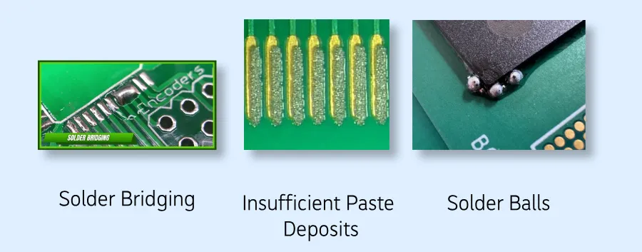
Implementing multilevel stencils requires calibrated printers with vision alignment for step registration. Initial runs test paste rheology, adjusting viscosity for optimal flow through varying depths. Electric engineers monitor transfer efficiency, targeting 75 to 125 percent volume for most joints. Common issues include insufficient paste on low steps due to squeegee skipping, resolved by increasing pressure or angle.
Stencil welding defects manifest as weak bonds causing flex during cleaning. Inspect welds visually and via ultrasound for voids. If bridging occurs on fine-pitch areas, thin those apertures further or add vents. Paste beading signals excess volume, prompting step-down redesigns. Cleaning regimens use targeted ultrasonics to preserve weld integrity without residue buildup.
For stencil welding processes, pre-weld fixturing aligns foils precisely. Post-weld annealing relieves stresses. Troubleshooting high step wear involves rotating print direction. These steps ensure consistent performance over production runs.
Related Reading: The Ultimate Guide to Step Stencil Manufacturing: Processes and Materials
Troubleshooting Common Defects in Multilevel Stencil Applications
Defects like tombstoning trace to uneven paste heights, where multilevel adjustments equalize volumes. Bridging in fine-pitch zones often stems from thick paste carryover, mitigated by step-downs. Insufficient solder on large pads causes head-in-pillow, addressed by boosting step heights. Engineers use 3D SPI to quantify variances, correlating to stencil features.
Gasketing failures at steps lead to smearing, fixed by optimizing snap-off and pressure. Weld-related issues show as stencil warping, prompting frame redesigns. Systematic root-cause analysis, from design to process, resolves most problems. Documenting fixes refines future iterations.
Case Study: Optimizing Mixed-Height Components
Consider a server board with 0.3mm pitch BGAs alongside electrolytic capacitors. Single-level stencils yielded 15 percent rework from bridging and voids. Switching to a stencil-welded multilevel design thinned BGA apertures and thickened cap pads. Prints achieved uniform heights, dropping defects to under 2 percent. Alignment tweaks and paste tweaks finalized the process. This case highlights stencil welding's role in high-reliability assemblies.
Conclusion
Multilevel solder paste stencils revolutionize SMT by enabling precise, component-specific paste deposition. Stencil welding enhances their durability for demanding production. Engineers gain actionable insights from IPC-7525 on design and IPC-7527 on printing criteria. Practical troubleshooting ensures peak performance. Adopting these tools elevates assembly quality and efficiency. Future trends point to even finer multilevel features for next-gen electronics.
FAQs
Q1: What are the benefits of multilevel stencils in PCB assembly?
A1: Multilevel stencils provide tailored solder paste volumes for diverse components, reducing bridging on fine-pitch parts and voids on larger pads. They cut changeover time in high-mix lines and improve yields per IPC-7527 guidelines. Electric engineers appreciate the single-print efficiency for complex boards.
Q2: How does stencil welding contribute to multilevel stencil performance?
A2: Stencil welding fuses foil layers for stable step structures, enduring high-cycle printing without delamination. It allows precise thickness variations unattainable otherwise. Troubleshooting focuses on weld inspection to prevent flexing issues during SMT.
Q3: When should electric engineers choose multilevel over single-level stencils?
A3: Opt for multilevel stencils on boards mixing fine-pitch ICs with power devices needing more paste. They excel in density-driven designs per IPC-7525. Single-level suffices for uniform components but compromises mixed-tech reliability.
Q4: What common troubleshooting steps apply to stencil welding multilevel stencils?
A4: Check weld integrity with magnification, adjust squeegee for step gasketing, and verify paste volume via SPI. Redesign abrupt transitions to avoid starvation. Regular cleaning preserves performance across runs.


