ALLPCB


Introduction
Lead-free PCB assembly has become the standard in electronics manufacturing due to global regulations restricting hazardous substances. Engineers face unique challenges when selecting components for these processes, as lead-free solders require higher reflow temperatures compared to traditional tin-lead alloys. Proper component selection ensures reliable solder joints, minimizes defects like tombstoning or head-in-pillow, and maintains long-term assembly integrity. This lead-free component selection guide focuses on practical strategies tailored for electric engineers, emphasizing compatibility, temperature ratings, and compliance. By prioritizing these factors early in the design phase, teams can avoid costly rework and production delays. Understanding the interplay between component properties and assembly conditions is crucial for success.
Why Lead-Free Assembly Demands Specialized Component Selection
The transition to lead-free assembly stems from environmental regulations that limit lead content in electronics. Lead-free solders, typically based on tin-silver-copper alloys, melt at higher temperatures and demand components capable of enduring elevated thermal profiles without degradation. Components not suited for these conditions can suffer from package cracking, delamination, or electrical failures during reflow. Electric engineers must evaluate lead-free component compatibility to match device specifications with process requirements, preventing issues like warpage or insufficient wetting. This selection process directly impacts yield rates and product reliability in high-volume production. Ignoring these aspects often leads to troubleshooting sessions that extend timelines unnecessarily.
Technical Principles Behind Lead-Free Component Challenges
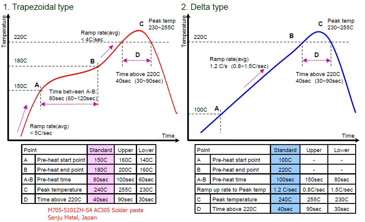
Lead-free reflow processes expose components to peak temperatures around those specified in industry standards, stressing plastic molding compounds and lead frames. Higher liquidus points mean longer time above liquidus, increasing risks of voiding or intermetallic compound formation at the solder interface. Component bodies must resist softening or outgassing, while terminations need finishes that promote reliable wetting without excessive dissolution. Thermal expansion mismatches between components and PCB substrates can exacerbate these issues during cooling. Engineers troubleshoot by analyzing reflow profiles against component datasheets, ensuring margins for process variations. These principles guide the lead-free component temperature rating assessments essential for robust assemblies.
JEDEC J-STD-020 outlines moisture/reflow sensitivity classifications that classify components based on their ability to withstand predefined reflow conditions.
Evaluating Lead-Free Component Temperature Ratings
Assessing lead-free component temperature rating starts with reviewing datasheet specifications for maximum reflow exposure. Components must tolerate peak body temperatures without exceeding their rated limits, typically verified through preconditioning tests. Plastic encapsulated devices require high glass transition temperatures in their molding compounds to avoid popcorn cracking from moisture vaporization. Engineers should cross-check ratings against actual oven profiles, accounting for conveyor speed and zone settings. Marginal ratings often reveal themselves in pilot runs through defects like lifted pads or incomplete reflow. Prioritizing components with proven high-temperature performance streamlines the lead-free component selection guide.
Inadequate temperature ratings manifest as troubleshooting challenges, such as charring on resistors or capacitors failing prematurely post-reflow. Select devices explicitly qualified for lead-free processes to mitigate these risks.
Ensuring Lead-Free Component RoHS Compliance
Lead-free component RoHS compliance verifies that devices meet restrictions on hazardous substances, particularly lead below specified thresholds. Manufacturers mark compliant parts with codes indicating finish and material composition, aiding procurement teams in verification. Non-compliant components introduce contamination risks during mixed assembly, potentially voiding certifications. Engineers confirm compliance through labeling and supplier declarations, avoiding exemptions that may not align with end-product needs. This step integrates seamlessly into component selection workflows, ensuring traceability from design to fabrication. Troubleshooting compliance issues often involves auditing supply chains for consistent documentation.
IPC/JEDEC J-STD-609 provides standardized marking for lead-free components, distinguishing finishes like matte tin from pure tin to support reliable identification.
Related Reading: Sustainable PCB Layout: Choosing Lead Free Components and Materials
Assessing Termination Finish and Compatibility
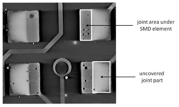
Lead-free component compatibility extends to termination finishes, where pure tin poses tin whisker risks over time. Matte tin or tin alloys with additives reduce whisker growth propensity while maintaining solderability. Engineers evaluate finish thickness and microstructure to predict long-term reliability in humid environments. Incompatible finishes lead to poor wetting, black pad syndrome, or excessive intermetallic buildup. Practical testing involves simulated aging followed by reflow trials to validate joint integrity. Selecting finishes balanced for assembly and field life prevents field failures traced back to component choices.
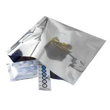
Managing Moisture Sensitivity in Lead-Free Assemblies
Moisture sensitivity levels dictate handling protocols to prevent reflow-induced damage. Components absorb ambient humidity, which expands rapidly at high temperatures, causing internal delamination. IPC/JEDEC J-STD-033 standardizes bagging, baking, and floor life limits based on classification. Engineers implement dry storage cabinets and verify indicators on moisture barrier bags before assembly. Troubleshooting moisture-related defects requires root cause analysis via cross-sections revealing voids or cracks. Integrating these practices into the lead-free component selection guide enhances overall process control.
Best Practices for Comprehensive Component Selection
Start component selection with a matrix evaluating temperature rating, MSL, finish type, and RoHS status against assembly profiles. Collaborate with suppliers for qualification data aligned with target processes. Conduct design for manufacturability reviews incorporating lead-free specifics, simulating reflow impacts on critical parts. Prioritize through-hole components with high-lead solders only if exemptions apply, favoring surface-mount for consistency. Pilot assemblies validate selections, allowing adjustments before full production. These practices form the core of an effective lead-free component selection guide.
IPC J-STD-001 specifies requirements for soldered assemblies, including criteria for lead-free materials and process verification.
Use diverse suppliers to mitigate shortages of high-reliability parts, always verifying lot traceability.
Common Pitfalls and Troubleshooting Insights
Overlooking lead-free component compatibility often results in tombstoning on fine-pitch devices due to uneven heating. Excessive peak temperatures from mismatched ratings cause capacitor failures, identifiable by bulging cases post-reflow. Tin whisker mitigation fails when pure tin finishes evade detection, leading to intermittent shorts years later. Moisture mishandling shows as white voids in X-rays, necessitating rebaking protocols. Engineers troubleshoot by correlating defect maps with component batches, refining selection criteria iteratively. Addressing these pitfalls proactively boosts first-pass yields significantly.
Related Reading: Sustainable Soldering: Choosing Lead-Free Alternatives for Eco-Friendly PCB Assembly
Conclusion
Effective component selection strategies for lead-free PCB assembly hinge on balancing thermal endurance, compliance, and material compatibility. Electric engineers who methodically assess temperature ratings, verify RoHS markings, and manage moisture risks achieve reliable, high-yield productions. Standards like those from IPC and JEDEC provide the framework for these decisions, minimizing troubleshooting needs. Adopting a structured lead-free component selection guide ensures assemblies withstand real-world stresses. Prioritizing these elements not only meets regulatory demands but also enhances product longevity. Teams ready to implement these practices position themselves for seamless transitions in modern manufacturing.
FAQs
Q1: What should electric engineers prioritize in lead-free component temperature rating?
A1: Focus on peak reflow tolerance and time-at-temperature from datasheets, ensuring alignment with process profiles. Verify through MSL preconditioning tests to catch vulnerabilities early. This prevents defects like delamination during assembly. Practical checks include thermal simulations for critical packages.
Q2: How do you confirm lead-free component RoHS compliance during procurement?
A2: Inspect markings per industry standards for codes indicating Pb-free status. Request material declarations from suppliers listing substance concentrations. Cross-verify against exemptions for your application. This step avoids contamination in mixed assemblies.
Q3: What are common lead-free component compatibility issues in PCB assembly?
A3: Issues include tin whiskers from pure tin finishes and poor wetting on mismatched terminations. Thermal mismatches cause warpage, while inadequate ratings lead to package failures. Troubleshoot with finish analysis and reflow trials.
Q4: Why is a lead-free component selection guide essential for engineers?
A4: It streamlines choices for temperature, MSL, and finishes, reducing defects and rework. Guides incorporate standards for consistent decisions across teams. This approach improves yields and reliability in production.
References
IPC/JEDEC J-STD-020E — Moisture/Reflow Sensitivity Classification. IPC/JEDEC, 2014
IPC/JEDEC J-STD-609A — Marking and Labeling of Components, PCBs and Solder Alloys. IPC/JEDEC, 2016
IPC/JEDEC J-STD-033D — Handling, Packing, Shipping and Use of Moisture/Reflow Sensitive Surface Mount Devices. IPC/JEDEC, 2018
IPC J-STD-001J — Requirements for Soldered Electrical and Electronic Assemblies. IPC, 2024