ALLPCB


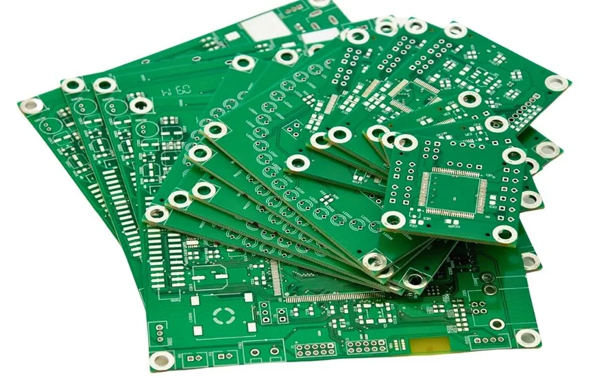
In the world of electronics, creating a sustainable PCB layout is more important than ever. If you're looking to design eco-friendly printed circuit boards (PCBs), choosing lead-free components and materials is a critical step. This means using lead-free solder, RoHS compliant components, lead-free finishes, and following lead-free PCB assembly practices. In this blog, we'll dive deep into why these choices matter, how to implement them, and the benefits they bring to your projects and the environment.
Why Choose Lead-Free Components and Materials for PCB Layout?
The shift to lead-free components and materials isn’t just a trend—it’s a necessity driven by environmental and health concerns. Lead, once a common material in electronics, is toxic and poses risks to both human health and the environment when improperly disposed of. Regulations like the Restriction of Hazardous Substances (RoHS) directive have pushed the industry toward safer alternatives, making lead-free options the standard for sustainable PCB design.
By opting for lead-free solder, RoHS compliant components, and lead-free finishes, you’re not only complying with global standards but also contributing to a cleaner planet. Plus, many industries now require lead-free PCB assembly to meet customer and regulatory demands. Let’s explore how to make these choices effectively for your next project.
Understanding Lead-Free Components and RoHS Compliance
Lead-free components are electronic parts manufactured without the use of lead in their construction or soldering process. These components are designed to meet RoHS standards, which restrict the use of hazardous substances like lead, mercury, and cadmium in electronic products. RoHS compliant components are essential for ensuring that your PCB layout aligns with international environmental regulations.
Choosing RoHS compliant components offers several advantages. First, it ensures that your product can be sold in markets with strict environmental laws, such as the European Union. Second, it reduces the risk of health issues for workers during manufacturing and for end-users if the product is mishandled or discarded. Common lead-free components include resistors, capacitors, and integrated circuits made with alternative materials like tin, silver, or copper alloys.
For example, a typical lead-free resistor might use a tin-silver-copper alloy for its terminals, ensuring good conductivity and durability without the environmental impact of lead. When selecting components, always check the manufacturer’s datasheet for RoHS compliance certification to confirm they meet the necessary standards.
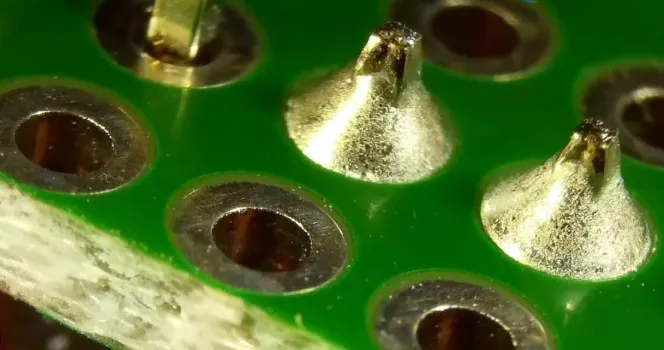
The Role of Lead-Free Solder in Sustainable PCB Assembly
Lead-free solder is a cornerstone of sustainable PCB assembly. Traditional solders often contained a mix of lead and tin (like 60/40 Sn-Pb solder), which provided excellent melting points and reliability. However, due to environmental concerns, lead-free solder alternatives, such as SAC305 (a tin-silver-copper alloy with 96.5% tin, 3% silver, and 0.5% copper), have become the industry standard.
Lead-free solder typically has a higher melting point, often around 217-220°C compared to 183°C for traditional leaded solder. This means your PCB materials and components must withstand higher temperatures during assembly. For instance, using substrates with a higher glass transition temperature (Tg), such as FR-4 with a Tg of 170°C or more, is crucial to prevent damage during soldering.
While lead-free solder can be more expensive and may require adjustments in your assembly process, the benefits are clear. It reduces toxic waste and aligns with RoHS requirements, making your products safer and more marketable. When designing your PCB layout, ensure that your soldering profiles and equipment are optimized for these higher temperatures to avoid issues like poor joint formation or thermal stress.
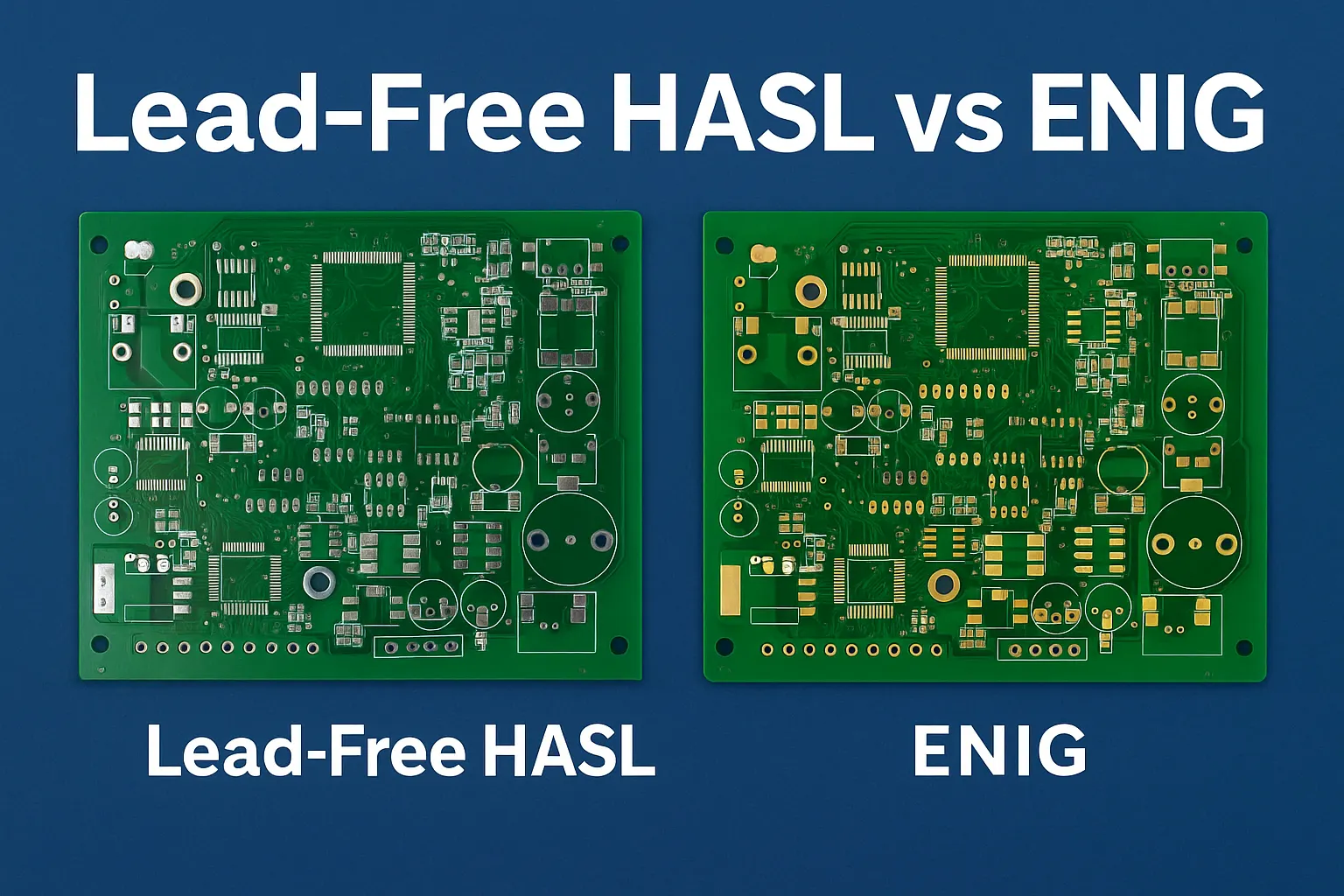
Selecting Lead-Free Finishes for PCB Durability and Compliance
The surface finish of a PCB plays a big role in its performance and sustainability. Lead-free finishes protect the copper traces on your board from oxidation and ensure reliable soldering. In the past, Hot Air Solder Leveling (HASL) with lead was a popular choice due to its low cost and ease of use. Today, lead-free HASL and other alternatives like Electroless Nickel Immersion Gold (ENIG), Immersion Silver (ImAg), and Organic Solderability Preservative (OSP) are widely used for sustainable PCB layouts.
Let’s break down a few popular lead-free finishes:
- Lead-Free HASL: This finish uses a tin-copper alloy instead of lead, providing a cost-effective option with good solderability. It’s ideal for simpler designs but may not be suitable for fine-pitch components due to uneven surface thickness.
- ENIG: This finish combines a layer of nickel with a thin gold coating, offering excellent corrosion resistance and flatness for high-density layouts. It’s perfect for complex designs with fine-pitch components.
- Immersion Silver (ImAg): A thin layer of silver provides good conductivity and solderability. It’s a cost-effective lead-free option but requires careful handling to avoid tarnishing.
Choosing the right lead-free finish depends on your PCB’s application, budget, and assembly requirements. For high-reliability applications like medical or aerospace devices, ENIG might be the best choice due to its durability, even though it costs more. For simpler consumer electronics, lead-free HASL can be a practical and eco-friendly option.
Best Practices for Lead-Free PCB Assembly
Lead-free PCB assembly requires careful planning to ensure reliability and compliance with environmental standards. Since lead-free materials often involve higher processing temperatures, your assembly process must be adapted to avoid issues like component damage or poor solder joints. Here are some best practices to follow:
- Choose Compatible Materials: Ensure that your PCB substrate, components, and solder are all compatible with lead-free assembly. For instance, use laminates with a higher thermal resistance (Tg above 170°C) to handle the elevated soldering temperatures.
- Optimize Reflow Profiles: Adjust your reflow oven settings to match the melting point of lead-free solder, typically around 217-220°C. A well-designed thermal profile prevents overheating and ensures strong solder joints. For example, a peak temperature of 245°C for 30-60 seconds is often recommended for SAC305 solder.
- Monitor Moisture Sensitivity: Lead-free assembly can increase the risk of moisture-related defects like popcorn cracking in components. Store moisture-sensitive devices in dry conditions and follow proper baking procedures before assembly.
- Inspect for Defects: Lead-free solder is more prone to issues like tin whiskers—tiny conductive filaments that can cause short circuits. Use high-magnification inspection tools to check for such defects post-assembly.
By following these steps, you can achieve a reliable lead-free PCB assembly process that meets RoHS standards and delivers high-quality results. Working with experienced manufacturing partners who specialize in lead-free processes can also help streamline your production and reduce errors.
Challenges and Solutions in Using Lead-Free Components and Materials
While the benefits of lead-free components and materials are undeniable, they do come with challenges. Understanding these hurdles and how to overcome them is key to a successful sustainable PCB layout.
Higher Costs: Lead-free solder and RoHS compliant components often cost more than their leaded counterparts. For instance, SAC305 solder can be 20-30% more expensive than traditional Sn-Pb solder due to the inclusion of silver. To manage costs, consider bulk purchasing or optimizing your design to use fewer components without sacrificing performance.
Thermal Stress: The higher melting points of lead-free solder can stress components and substrates, leading to cracks or delamination. Using materials with better thermal stability, such as high-Tg FR-4 or polyimide, can mitigate this risk.
Reliability Concerns: Lead-free solder joints may be more brittle, increasing the risk of failure under mechanical stress or thermal cycling. To improve reliability, incorporate design features like larger pads or additional vias to distribute stress more evenly across the board.
By anticipating these challenges and implementing the right solutions, you can ensure that your lead-free PCB design performs well while staying environmentally friendly.
Benefits of Sustainable PCB Layout with Lead-Free Materials
Adopting a sustainable PCB layout with lead-free components and materials offers numerous advantages beyond just regulatory compliance. Here are some key benefits:
- Environmental Impact: Reducing hazardous materials like lead helps minimize electronic waste pollution, protecting ecosystems and human health.
- Market Access: Many global markets, especially in Europe and Asia, require RoHS compliance for electronic products. Using lead-free materials ensures your products can be sold worldwide.
- Brand Reputation: Companies that prioritize sustainability often gain a positive reputation among customers and partners, enhancing trust and loyalty.
- Future-Proofing: As regulations become stricter, adopting lead-free practices now prepares your business for upcoming changes in environmental laws.
For example, a consumer electronics company that switches to lead-free PCB assembly can market its products as eco-friendly, appealing to environmentally conscious buyers and gaining a competitive edge.
Conclusion: Building a Greener Future with Lead-Free PCB Design
Creating a sustainable PCB layout by choosing lead-free components and materials is a powerful way to contribute to a greener future. From using RoHS compliant components and lead-free solder to selecting the right lead-free finishes, every decision in the design and assembly process matters. While challenges like higher costs and thermal stress exist, the benefits of compliance, market access, and environmental responsibility far outweigh the drawbacks.
By following best practices for lead-free PCB assembly and staying informed about industry standards, you can design high-quality, eco-friendly PCBs that meet both technical and regulatory requirements. Start incorporating these sustainable practices into your next project and take a step toward a cleaner, safer world.