 ALLPCB


Introduction
In high-frequency PCB design, maintaining signal integrity and minimizing electromagnetic interference stands as a primary challenge for electrical engineers working on RF applications. PCB edge plating RF techniques emerge as a vital solution to contain radiated emissions and ensure robust ground connections across multiple layers. These methods involve applying conductive material along the board edges, creating a continuous shield that bridges ground planes and enhances overall electromagnetic compatibility. For microwave circuits operating at elevated frequencies, such edge plating proves essential to prevent field leakage that could degrade performance. This article explores advanced PCB edge plating techniques tailored for RF and microwave environments, drawing on established engineering principles to guide design decisions.
What Is PCB Edge Plating and Why It Matters for RF Applications
PCB edge plating refers to the process of depositing a conductive layer, typically copper, onto the vertical sidewalls of a printed circuit board. This technique extends the metallization beyond traditional traces and pads to encase the board perimeter, forming either a full wraparound or selective coverage. In RF PCB edge plating, the primary goal centers on interconnecting ground planes from top to bottom layers, thereby suppressing edge radiation and crosstalk. Without proper edge treatment, high-frequency signals propagate as microstrip or stripline modes, where fringing fields escape the board edges, leading to unintended coupling with nearby structures.
The relevance intensifies in microwave applications, where wavelengths approach board dimensions, amplifying radiation risks. PCB edge plating microwave configurations act as a Faraday-like barrier, reflecting energy back into the substrate and maintaining controlled impedance. Engineers benefit from improved electromagnetic compatibility, reduced susceptibility to external noise, and simplified integration with enclosures. According to IPC-2221 guidelines on printed board design, perimeter edge plating supports these functions by specifying requirements for edge metallization integrity.
Technical Principles of Edge Plating in High-Frequency Environments
At the core of PCB edge plating RF effectiveness lies its ability to provide a low-impedance return path for high-frequency currents. Skin effect confines currents to the conductor surface, making uniform plating crucial for minimizing losses in microwave signals. The plated edge creates a continuous conductive path that shorts adjacent ground planes, eliminating slot antennas formed by disjointed pours. This mechanism suppresses cavity modes and parallel-plate resonances that plague multilayer stacks in RF designs.
Electromagnetic field confinement occurs as the plating reflects transverse electric and magnetic fields, preventing spillover beyond the board boundary. In high-frequency PCB design, this translates to preserved characteristic impedance for transmission lines adjacent to edges. Plating also mitigates via stub effects by offering alternative stitching points along the perimeter. Fabrication processes begin with panelization, where boards remain connected via tabs during plating to ensure sidewall access.
Advanced simulations reveal that edge plating reduces far-field emissions by orders of magnitude compared to unplated edges. The technique proves particularly valuable in dense RF layouts with edge-mounted connectors, where direct chassis grounding becomes feasible.
Types of Advanced PCB Edge Plating Techniques
Several advanced techniques adapt PCB edge plating for RF demands, each suited to specific microwave scenarios. Full edge plating coats the entire perimeter, ideal for comprehensive shielding in standalone RF modules. Partial or selective plating targets critical sections, such as near high-power amplifiers, conserving material while focusing on radiation hotspots. Wrapping plating extends the copper layer around corners, ensuring seamless coverage despite routing imperfections.
Castellated edge plating, featuring half-moon cutouts, supports modular RF assemblies like front-end modules. These half-vias allow soldering to daughterboards while maintaining ground continuity. Tooth or serrated edges represent a variation, providing mechanical interlocking alongside electrical shielding. In high-frequency PCB design, combining these with ground via fences amplifies suppression of surface waves.
Panel-based fabrication enables precise control, with temporary tabs preserving plating uniformity before singulation. Electroless seeding followed by electrolytic deposition builds the necessary thickness for durability under thermal cycling.
Design and Implementation Best Practices for RF PCB Edge Plating
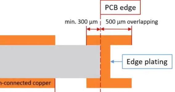
Effective high-frequency PCB design incorporates edge plating early in the layout phase to avoid rework. Define plating regions using dedicated polygons assigned to ground nets, extending slightly beyond the board outline for fabrication tolerance. Establish clearance rules separating edge copper from signal traces, preventing shorts while allowing pour connectivity to inner layers. Remove solder mask along plated edges to expose copper for enclosure contact and soldering.
In PCB edge plating RF workflows, integrate with impedance-controlled stacks using low-loss dielectrics. Position edge plating away from sensitive RF ports, yet close enough for stitching vias every few millimeters. Specify fabrication notes requesting sidewall plating with adequate overlap onto surface layers for adhesion strength. Verify continuity through test coupons on panels, ensuring plating wraps fully around edges.
For microwave applications, align plating with enclosure seams to form a continuous shield. Avoid abrupt terminations that could radiate; instead, use gradual transitions or slots with bridging tabs.
IPC-6018 outlines performance criteria for such high-frequency boards, emphasizing plating uniformity and adhesion in microwave environments.
Manufacturing Considerations and Quality Assurance
Transitioning from design to production demands clear communication of PCB edge plating microwave requirements. Panelization with strategic tabs maintains structural integrity during plating, allowing access to sidewalls via immersion in baths. Post-plating routing severs tabs cleanly, leaving plated edges intact. Inspect for voids, cracks, or delamination using cross-section microscopy, focusing on wraparound coverage.
Surface preparation, including edge beveling, enhances adhesion by increasing plating surface area. Final finishes like immersion tin protect against oxidation without compromising RF performance. Quality metrics include continuity resistance below thresholds and thickness uniformity across heights.
In RF applications, thermal management benefits from edge plating's extended copper area, dissipating heat to chassis grounds.
Troubleshooting Common Issues in RF Edge Plating
Engineers often encounter plating inconsistencies in high-frequency PCB design, such as incomplete sidewall coverage from poor panel handling. Over-etching during singulation can thin edges, raising impedance discontinuities. Mitigate by specifying conservative tab dimensions and post-plate inspections.
Signal leakage persists if ground pours fail to connect through vias; resolve with dense stitching arrays tied to edge nets. Mechanical stress from mismatched CTE in multilayer stacks risks cracking; select compatible laminates per application needs.
IPC-2228 provides sectional guidance for RF/microwave board design, including edge treatments to avoid these pitfalls.
Conclusion
Advanced PCB edge plating techniques elevate RF PCB performance by delivering superior shielding, ground integrity, and EMI control. From full perimeter wraps to castellated modules, these methods address the unique demands of high-frequency and microwave circuits. Electrical engineers achieve reliable designs by adhering to structured layout practices, precise fabrication specs, and standard-compliant verification. Integrating PCB edge plating RF early ensures compact, efficient boards ready for demanding applications. Future iterations may refine processes for even higher frequencies, but current approaches set a solid foundation.
FAQs
Q1: What role does PCB edge plating play in high-frequency PCB design?
A1: PCB edge plating RF connects ground planes across layers, containing fringing fields and reducing emissions in microwave circuits. It forms a shield that prevents edge radiation, maintaining signal integrity for transmission lines. Design it as polygon pours extending to edges, with clearances to signals. Fabrication requires panel tabs for uniform deposition. This technique aligns with IPC standards for reliable performance.
Q2: How does PCB edge plating microwave improve EMI shielding?
A2: In PCB edge plating microwave setups, the continuous copper sidewall reflects electromagnetic energy back into the board, suppressing cavity modes. It bridges disjointed grounds, eliminating slot radiators common in multilayers. Best practices include solder mask openings for enclosure contact and via stitching. This enhances EMC without bulky external shields, ideal for compact RF modules.
Q3: What are best practices for implementing RF PCB edge plating in layout?
A3: Assign edge plating to dedicated ground nets using extended pours in high-frequency PCB design. Set negative outline clearances for overhang and define gaps to connectors. Remove mask on edges for conductivity. Include fab notes for thickness and overlap. Verify with simulations for field confinement.
Q4: When should engineers use castellated edges in PCB edge plating RF?
A4: Castellated PCB edge plating RF suits modular designs like RF front-ends, providing half-vias for soldering to carriers. It maintains shielding while enabling mechanical alignment. Ensure plating covers semicircles fully for continuity. Avoid in full-board shielding where solid edges suffice.
References
IPC-2221B — Generic Standard on Printed Board Design. IPC.
IPC-6018D — Qualification and Performance Specification for High Frequency (Microwave) Printed Boards. IPC.
IPC-2228 — Sectional Design Standard for High Frequency (RF/Microwave) Printed Boards. IPC.


