 ALLPCB


Introduction
Electronic hobbyists often push the boundaries of PCB design to pack more functionality into smaller spaces, making blind and buried vias essential for multilayer home projects. These vias enable higher component density without wasting surface area on through-hole connections, but they introduce unique challenges during fabrication and assembly. PCB via problems like cracking or opens can turn a promising prototype into a frustrating failure, especially when working with affordable manufacturing services. Understanding these pitfalls allows hobbyists to troubleshoot effectively and improve reliability. This guide focuses on practical insights for DIY PCB troubleshooting, drawing from standard manufacturing principles to help you avoid common blind via repair headaches and buried via issues. By mastering these concepts, you can elevate your home PCB projects to professional levels.
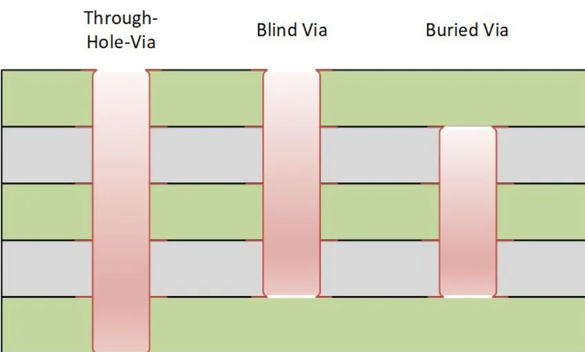
What Are Blind and Buried Vias and Why Do They Matter in Home PCBs?
Blind vias connect an outer layer to one or more inner layers without penetrating the entire board thickness, while buried vias link only inner layers, remaining completely hidden from the surfaces. These structures save valuable real estate on dense boards, allowing hobbyists to route signals more efficiently in projects like compact microcontrollers or sensor arrays. In home PCBs, they matter because modern designs demand tighter layouts, but their partial or hidden nature makes inspection and repair far trickier than standard through vias. Poorly executed blind or buried vias lead to intermittent failures that are hard to diagnose without specialized tools. For electronic hobbyists, incorporating them opens doors to advanced layouts but requires awareness of fabrication tolerances to prevent buried via issues. Ultimately, they boost performance when done right, enabling sleeker prototypes without compromising functionality.
Common Causes of PCB Via Problems in Blind and Buried Vias
One primary cause of PCB via problems stems from plating defects, where incomplete copper deposition creates voids or thin walls in the via barrel, leading to high resistance or outright opens. During electroplating, inadequate parameters like poor electrolyte agitation or high aspect ratios prevent uniform coverage, especially in blind vias with tapered walls from laser drilling. Thermal fatigue exacerbates this, as coefficient of thermal expansion mismatches between copper plating and the dielectric material cause cracking during reflow soldering or operational heat cycles. Misregistration during sequential lamination steps often results in the via missing its target pad, creating non-contact failures that are invisible from the surface. Delamination at the via-dielectric interface, triggered by moisture absorption or weak adhesion, further compounds buried via issues by separating layers entirely. According to IPC-6012 standards, maintaining minimum plating thickness is crucial to mitigate these risks in multilayer boards.
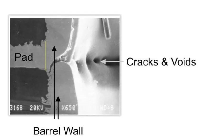
Drill smear residue or insufficient etch-back also leads to poor bottom metallization in blind vias, where the copper fails to adhere properly to the landing pad. High aspect ratios, exceeding 1:1 for microvias, hinder plating uniformity and increase mechanical stress concentrations. In home PCB contexts, using services without tight process controls amplifies these issues, as sequential builds add lamination cycles that heighten warpage risks.
DIY PCB Troubleshooting Techniques for Blind and Buried Vias
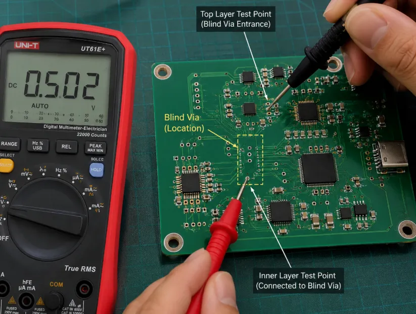
Start your DIY PCB troubleshooting with basic electrical testing using a multimeter to check continuity across nets involving blind or buried vias, identifying opens or high resistance early. Apply power and probe for voltage drops under load to detect intermittent buried via issues that only appear during operation. Visual inspection under magnification reveals surface anomalies like dimples or cracks on blind via openings, though buried ones require more ingenuity. For deeper analysis, perform a gentle thermal cycle test by heating the board evenly with a heat gun or oven to simulate reflow, then retest continuity for emerging faults. Cross-sectioning a scrap board sample with a fine saw and polish provides direct views of internal plating quality, mimicking IPC-A-600 acceptability criteria without advanced equipment. Document findings with photos to correlate failures with design choices.
If electrical tests pass but performance lags, inspect for signal integrity problems using an oscilloscope on high-speed traces, where via stubs in blind structures cause reflections. Acoustic tapping around via areas can hint at delamination in buried vias, producing dull sounds compared to solid regions. These hobbyist-friendly steps pinpoint PCB via problems efficiently before escalating to redesigns.
Practical Solutions and Blind Via Repair for Hobbyists
For minor plating voids accessible on blind vias, clean the opening with isopropyl alcohol and flux, then fill with conductive epoxy using a syringe for reliable z-axis conductivity. Cure the epoxy per manufacturer instructions, typically at low heat, and verify with continuity tests to ensure current handling matches original specs. Avoid overfilling to prevent shorts to adjacent layers. Jumper wires soldered across failed surface connections serve as a quick workaround for outer blind via issues, insulated with conformal coating afterward. However, buried via issues demand prevention over repair, as accessing inner layers risks board destruction. IPC-2221 guidelines emphasize design rules like adequate annular rings to reduce these repair needs from the start.
In cases of thermal cracking, backdrilling the via stub carefully with a small CNC or hand drill removes damaged sections, followed by conductive fill, though precision is key to avoid nearby traces. Always test repaired boards under accelerated stress, like repeated soldering irons, to validate longevity.
Best Practices to Prevent Buried Via Issues and Enhance Reliability
Adopt staggered via configurations over stacked ones to distribute thermal stress and improve plating uniformity, especially in hobbyist multilayer designs. Limit blind via aspect ratios to under 1:1 and ensure drill depths match layer stackups precisely in your design files. Select high-Tg dielectric materials to withstand reflow temperatures and minimize CTE-induced cracking. Specify minimum copper plating thickness in fab quotes, aligning with industry benchmarks for Class 3 reliability. Stagger via placements by at least 0.2 mm to prevent overlapping stress fields during lamination.
Incorporate generous annular rings around vias and avoid clustering them near board edges where warpage peaks. Perform design rule checks for via-to-via spacing and simulate thermal profiles if possible. These steps drastically cut buried via issues in home PCBs.
Real-World Insights from Hobbyists Troubleshooting Sessions
Consider a common scenario where a hobbyist's four-layer motor driver board exhibited intermittent power delivery after assembly. Continuity tests revealed opens in buried vias linking ground planes, traced to delamination from excessive lamination cycles in the fab process. Cross-sectioning confirmed poor adhesion, resolved by redesigning with fewer layer transitions and staggered vias. In another case, blind vias in a sensor prototype cracked during hand soldering due to rapid heat ramps; slowing the process and adding thermal reliefs fixed it. These examples highlight how DIY PCB troubleshooting uncovers design-fab mismatches early. Proactive stackup reviews prevent recurrence.
Conclusion
Mastering blind and buried vias transforms home PCB projects from trial-and-error to reliable successes, sidestepping PCB via problems through informed design and troubleshooting. Key takeaways include prioritizing low aspect ratios, quality plating, and staggered layouts while leveraging simple tests like continuity and thermal cycling. Hobbyists equipped with these strategies can tackle blind via repair confidently and minimize buried via issues. Reference standards like IPC-6012 and IPC-A-600 during fab selection for consistent results. Embrace these practices to build denser, durable boards that perform under real-world stresses.
FAQs
Q1: What are the most frequent PCB via problems in blind vias for DIY projects?
A1: Blind vias often suffer from plating voids, thermal cracking, and misregistration, leading to opens or high resistance. These arise from high aspect ratios or poor fab controls. DIY PCB troubleshooting starts with multimeter checks and visual magnification to spot issues early. Addressing them via conductive fills restores function reliably.
Q2: How can hobbyists perform effective DIY PCB troubleshooting for buried via issues?
A2: Use continuity mapping and thermal stress tests to detect buried via issues without dissection. Magnified inspection and voltage drop measurements under load reveal hidden faults. Cross-section samples from prototypes confirm plating quality per acceptability criteria. Prevention through staggered designs outperforms reactive fixes.
Q3: Is blind via repair feasible at home without professional tools?
A3: Yes, conductive epoxy fills repair accessible blind via plating defects effectively after cleaning. Verify with post-cure continuity tests and avoid high-current applications. For deeper cracks, jumper alternatives work temporarily. Design adherence to via guidelines minimizes repair needs altogether.
Q4: What design tips prevent common buried via issues in multilayer home PCBs?
A4: Opt for staggered vias, low aspect ratios under 1:1, and high-Tg materials to combat stress and delamination. Ensure precise stackups and minimum plating specs in orders. These practices align with reliability standards, reducing failures in dense hobbyist layouts.
References
IPC-6012E — Qualification and Performance Specification for Rigid Printed Boards. IPC, 2017
IPC-A-600K — Acceptability of Printed Boards. IPC, 2020
IPC-2221B — Generic Standard on Printed Board Design. IPC, 2012


