 ALLPCB


Introduction
Solder paste plays a pivotal role in surface mount technology assembly, serving as the foundational material for creating reliable electrical interconnections on printed circuit boards. Engineers rely on it to deposit precise amounts of solder alloy and flux onto pads, which then reflows to form strong joints between components and the PCB. Understanding solder paste types, solder paste properties, and solder paste application methods ensures consistent yield and minimizes defects like bridging or voids. Proper solder paste storage and adherence to solder paste reflow profiles further enhance assembly success. This article delves into these aspects with a practical focus, helping electric engineers troubleshoot and optimize their processes. By mastering these elements, teams can achieve higher reliability in high-volume production.
What Is Solder Paste and Why It Matters
Solder paste consists of microscopic solder alloy particles suspended in a flux medium, typically making up 85 to 92 percent metal by weight. The flux activates during heating to remove oxides, promote wetting, and facilitate alloy melting into a liquidus state. Without quality solder paste, assemblies suffer from poor joint formation, leading to failures in functionality or long-term reliability. In PCB assembly lines, it directly impacts first-pass yield, as inconsistencies in deposition cause rework. Electric engineers must select pastes aligned with board complexity, component pitch, and environmental requirements. Ultimately, solder paste bridges design intent and manufacturing execution, making its characteristics non-negotiable for robust electronics.
Solder Paste Types
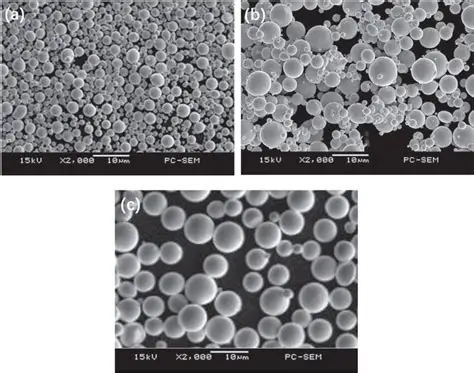
Solder paste types vary primarily by alloy composition, flux classification, and powder particle size, each suited to specific assembly challenges. Leaded pastes, such as those with Sn63Pb37 alloy, offer lower melting points around 183 degrees Celsius and excellent flow, ideal for prototyping or legacy systems. Lead-free alternatives like SAC305 dominate modern production, with higher melting points near 217 degrees Celsius to comply with environmental regulations. Flux types include no-clean formulations that leave benign residues and water-soluble options requiring post-reflow cleaning to prevent corrosion. Powder sizes follow classifications in J-STD-005, where Type 3 features particles from 25 to 45 microns for standard SMT, Type 4 suits finer pitches at 20 to 38 microns, and Type 5 enables ultra-fine features below 25 microns. Selecting the right combination prevents issues like solder balling in high-density boards.
Engineers often troubleshoot by matching paste type to stencil thickness and aperture design. For instance, coarser Type 3 paste releases cleanly from thicker stencils, while finer types reduce bridging on 0.3 millimeter pitches. Hybrid pastes blending alloy variants address mixed-technology assemblies. Always verify compatibility with reflow equipment to avoid incomplete coalescence.
Solder Paste Properties
Key solder paste properties include viscosity, thixotropy, slump resistance, tackiness, and metal load percentage, all critical for printability and joint quality. Viscosity measures flow resistance, typically 400,000 to 800,000 poise, ensuring stability during storage yet shear-thinning for stencil release. Thixotropy allows the paste to liquefy under squeegee pressure and reform structure post-print, preventing slumping off pads. Slump tests evaluate resistance to flow under gravity, vital for fine-pitch applications where excess spread causes shorts. Tackiness holds components in place pre-reflow, quantified by probe force measurements. High metal load, around 90 percent, maximizes joint volume but demands precise rheology to avoid voids.
These properties interlink during processing; poor thixotropy leads to solder beading, while inadequate tack results in tombstoning. Engineers assess via standard tests like those in J-STD-005, correlating lab data to production SPI results. Environmental factors, such as humidity, alter properties, necessitating controlled conditions. Optimizing these ensures uniform deposits across panels.
Solder Paste Application Methods
Stencil printing remains the dominant solder paste application method, using a laser-cut metal stencil to transfer paste via squeegee blades. The process involves aligning the stencil to the PCB, flooding paste across apertures, and snapping off cleanly with controlled pressure, speed, and snap-off distance. Typical parameters include 20 to 40 millimeters per second squeegee speed and 45 to 60 degree blade angle for optimal fill and release. IPC-7527 provides visual criteria for deposit quality, such as height uniformity and absence of bridging. For prototypes or repairs, needle dispensing offers precision on irregular pads, though slower for volume. Jetting dispenses micro-deposits without contact, ideal for 01005 components.
Troubleshooting print defects starts with gasket checks for stencil wear and paste agitation to maintain homogeneity. Over-printing signals excessive volume, fixed by reducing stencil thickness or gapping. Under-fill often traces to worn squeegees or dry paste, resolved by pre-wet floods. Vision systems verify volume post-print, correlating to X-ray for voids.
Solder Paste Storage and Handling
Proper solder paste storage extends usability and preserves properties, typically requiring refrigeration at 2 to 10 degrees Celsius in sealed jars. Shelf life ranges from 3 to 12 months unopened, depending on flux type, with no-clean pastes lasting longer due to stable chemistry. Avoid freezing unless specified, as cycles degrade rheology. Before use, allow natural thaw to room temperature over 4 to 8 hours to prevent condensation-induced separation. Agitate gently post-thaw to remix settled powder, checking for anomalies like hardening.
Handling best practices include first-in-first-out inventory, humidity below 60 percent, and dedicated tools to avoid contamination. Opened paste loses viability quickly at ambient temperatures, often within hours, prompting discard after shifts. Engineers track via labels and logs, correlating storage lapses to defect spikes like head-in-pillow. Climate-controlled environments yield consistent performance.
Solder Paste Reflow Profiles
Solder paste reflow profiles define heating zones to activate flux, melt alloy, and form intermetallics without damaging components. Standard profiles feature preheat (150 to 180 degrees Celsius for 60 to 120 seconds), soak (for flux activation), reflow above liquidus (60 seconds minimum at 220 to 260 degrees Celsius peak), and rapid cool. Lead-free pastes demand higher peaks per J-STD-020 classifications, with time above liquidus tailored to alloy. Profile development uses thermocouples on test boards, verifying ramp rates below 3 degrees Celsius per second to minimize thermal shock.
Troubleshooting deviant profiles involves oven zoning and nitrogen atmospheres to reduce oxidation. Excessive soak promotes flux char, while short reflow leaves dull joints. SPI and post-reflow AOI guide adjustments, ensuring peak temperatures align with paste specs.
Best Practices and Troubleshooting in PCB Assembly
Implement inline SPI after printing to catch volume variances early, adjusting squeegee pressure for 75 to 125 percent pad coverage. Mix paste batches consistently, using planetary mixers for homogeneity. For fine-pitch, elect Type 4 or 5 pastes with low slump. Common defects like bridging resolve via stencil polishing or reduced snap-off; voids from flux entrapment improve with longer soaks or low-residue fluxes.
Tombstoning, often from uneven heating, counters with symmetric pad designs and profiled preheats. Solder beading links to high oxide in powder, fixed by fresh paste. Document process windows per IPC guidelines, training operators on visual cues. These steps boost yields above 99 percent.
Conclusion
Mastering solder paste types, properties, application methods, storage, and reflow profiles empowers electric engineers to deliver defect-free PCB assemblies. Practical attention to these elements minimizes rework and enhances reliability. By aligning selections with process capabilities and standards, production scales efficiently. Troubleshooting rooted in data-driven adjustments sustains quality. Ultimately, informed handling of solder paste transforms potential pitfalls into predictable success.
FAQs
Q1: What are the main solder paste types for PCB assembly?
A1: Solder paste types include leaded and lead-free alloys, with flux variants like no-clean or water-soluble, and powder sizes from Type 3 to Type 5 per J-STD-005. Type 3 suits general SMT, while finer types handle high-density boards. Selection depends on pitch and reflow compatibility to avoid defects. Proper choice ensures clean release and strong joints.
Q2: How do solder paste properties affect application?
A2: Solder paste properties such as viscosity and thixotropy dictate print quality, with optimal ranges preventing slump or beading. High tack secures components pre-reflow. Engineers test slump and tack to match stencil processes. Deviations cause bridging, resolved by agitation or type swaps. Consistent properties yield uniform deposits.
Q3: What are best solder paste application methods?
A3: Stencil printing dominates solder paste application methods, using squeegees for precise volume transfer per IPC-7527 criteria. Dispensing aids low-volume work. Key parameters include speed and pressure for clean snaps. SPI verifies results, troubleshooting wear or dryness. This ensures reliable pad coverage across panels.
Q4: How should solder paste storage impact reflow profiles?
A4: Solder paste storage at 2 to 10 degrees Celsius preserves rheology for consistent reflow profiles. Improper thaw alters flow, risking voids. Align profiles to J-STD-020 for peak temps. Fresh paste enables standard soaks and cools. Monitor via logs to link handling to joint quality.
References
J-STD-005 — Requirements for Soldering Pastes. IPC
IPC-7527 — Requirements for Solder Paste Printing. IPC
IPC/JEDEC J-STD-020E — Moisture/Reflow Sensitivity Classification of Nonhermetic Solid State Surface Mount Devices. JEDEC, 2014


