 ALLPCB


High-reliability printed circuit boards must perform consistently under demanding conditions where ordinary designs would fail. Engineers working in sectors that require uninterrupted operation focus on every aspect of the board from material choice through final layout. PCB design for extreme environments therefore emphasizes prevention of mechanical stress, thermal cycling, and electrical degradation. Robust PCB design techniques integrate these considerations early in the development cycle to reduce the likelihood of field failures. High-reliability PCB layout guidelines translate these principles into concrete spacing, trace, and via decisions that maintain integrity over extended service life.
Why High-Reliability PCB Design Matters
Extreme operating conditions introduce multiple simultaneous stresses that accelerate common failure modes. Temperature swings cause differential expansion between copper and substrate layers, leading to cracking or delamination if the stack-up is not properly balanced. Vibration and shock transmit mechanical energy that can fatigue solder joints and copper traces. Moisture ingress promotes corrosion and electrochemical migration between conductors. PCB material selection for reliability directly influences how well the board resists these combined effects. Minimizing PCB failure risks therefore requires a systematic approach that begins with application requirements and proceeds through material qualification and layout verification.
Engineering Mechanisms Behind PCB Failures
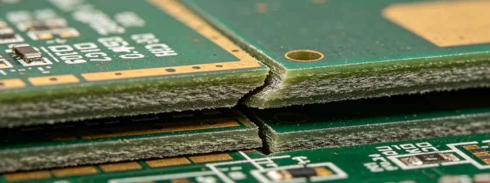
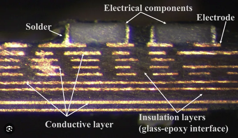
Thermal expansion mismatch remains one of the primary drivers of mechanical damage in multilayer boards. When the coefficient of thermal expansion differs significantly between copper and dielectric layers, repeated cycling generates shear stresses at interfaces. These stresses concentrate at vias and component pads, eventually producing barrel cracking or pad lift-off. Moisture absorption adds another dimension because absorbed water expands during reflow or high-temperature operation, creating internal pressure that can cause blistering or delamination. Electrical failures often stem from insulation degradation under high voltage or from dendritic growth when ionic contamination combines with humidity. Understanding these mechanisms allows designers to select materials whose properties remain stable across the expected temperature and humidity range.
Material Selection for Long-Term Stability
Substrate choice forms the foundation of any high-reliability design. Laminates with low moisture absorption and controlled coefficient of thermal expansion reduce the magnitude of internal stresses during temperature excursions. Glass transition temperature must remain above the maximum operating temperature to preserve mechanical rigidity. Copper foil thickness and surface treatment also affect adhesion and current-carrying capability under thermal load. When boards will experience repeated reflow or wave soldering, the laminate must withstand multiple thermal excursions without degradation. These considerations guide the initial stack-up definition before any layout work begins.
Related Reading: Material Matters: Choosing the Right Substrate for DFM in Flex PCBs
High-Reliability PCB Layout Guidelines
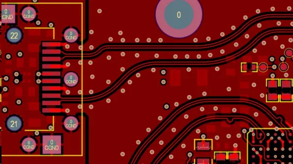
Trace routing and via placement must accommodate both electrical and mechanical requirements. Wider traces and larger via pads distribute current and reduce localized heating, while adequate spacing between conductors prevents arcing under high voltage. Placing sensitive traces away from board edges and mounting holes minimizes exposure to mechanical flexure. Thermal relief patterns around pads connected to large copper planes help control heat flow during soldering without compromising electrical performance. Symmetric placement of components and balanced copper distribution on opposite sides of the board reduce the risk of warpage during manufacturing and operation. These layout decisions collectively contribute to minimizing PCB failure risks throughout the product life cycle.
Related Reading: PCB Layout Design for EMI/EMC Compliance: Best Practices
Robust PCB Design Techniques for Extreme Environments
Designers apply additional techniques when boards must survive vibration, shock, or corrosive atmospheres. Increasing the number of mounting holes and using reinforced edge connectors improves mechanical attachment. Conformal coatings or potting compounds provide environmental protection once the board is assembled, yet the underlying layout must still allow for coating thickness and outgassing. For applications involving rapid temperature changes, designers incorporate thermal vias and heat-spreading planes to equalize temperatures across the board. Redundant signal paths or increased conductor cross-sections add margin against partial degradation. Each of these techniques builds on the material and layout foundation to create a board capable of sustained performance.
Practical Implementation and Verification
After completing the initial layout, simulation tools help identify potential stress concentrations before prototypes are built. Finite-element analysis of the board under expected thermal and mechanical loads reveals areas where additional reinforcement or layout changes may be beneficial. Prototype testing under accelerated conditions then validates the design choices. IPC-6012E provides acceptance criteria for rigid printed boards that include requirements for thermal stress testing and dimensional stability. Boards that meet these criteria demonstrate the necessary margin for high-reliability applications. Documentation of material lot numbers and process parameters further supports traceability and future design iterations.
Conclusion
High-reliability PCB design integrates material properties, layout geometry, and manufacturing considerations into a single coherent strategy. By addressing thermal expansion, moisture effects, and mechanical stresses at every stage, engineers create boards that maintain performance when ordinary designs would fail. Systematic application of high-reliability PCB layout guidelines and robust PCB design techniques reduces the incidence of field failures and extends service life. The result is a board that meets the demanding requirements of extreme environments while remaining manufacturable and cost-effective.
FAQs
Q1: What factors most influence PCB design for extreme environments?
A1: Material selection, stack-up symmetry, and trace geometry together determine how well a board withstands combined thermal, mechanical, and environmental stresses. Engineers evaluate coefficient of thermal expansion, moisture absorption, and glass transition temperature early in the process. Layout decisions such as via placement and copper balance then translate these material properties into reliable performance. Following established high-reliability PCB layout guidelines helps ensure consistent results across production lots.
Q2: How does PCB material selection for reliability affect long-term performance?
A2: The chosen laminate must maintain dimensional stability and electrical insulation across the full operating temperature and humidity range. Low moisture absorption reduces the risk of blistering during thermal excursions, while an appropriate glass transition temperature preserves mechanical strength. These properties directly influence the board’s ability to survive repeated cycling without delamination or cracking. Proper material qualification therefore forms the basis for minimizing PCB failure risks.
Q3: What layout practices support robust PCB design techniques under vibration?
A3: Increasing the number and size of mounting points, using wider traces near mechanical interfaces, and balancing copper distribution reduce flexure-induced fatigue. Avoiding placement of critical traces near board edges or large cutouts further protects against stress concentration. These measures complement component-level reinforcement and help maintain electrical continuity during mechanical shock events.
Q4: How can designers minimize PCB failure risks during thermal cycling?
A4: Symmetric stack-ups, thermal relief patterns, and strategic placement of thermal vias help equalize expansion across the board. Selecting laminates with controlled coefficient of thermal expansion matching the expected environment reduces shear stress at interfaces. Verification against industry standards such as JEDEC J-STD-020E confirms that the assembly process itself will not introduce latent defects that later manifest under field conditions.
References
IPC-6012E — Qualification and Performance Specification for Rigid Printed Boards. IPC, 2017
JEDEC J-STD-020E — Moisture/Reflow Sensitivity Classification. JEDEC, 2014
IPC-A-600K — Acceptability of Printed Boards. IPC, 2020





