 ALLPCB


Printed Circuit Boards (PCBs) are the backbone of modern electronics, but even small defects during manufacturing can lead to significant drops in yield, increased costs, and unreliable products. So, what are the common PCB defects that affect manufacturing yield? Some of the most frequent issues include microcracks, bubbles, delamination, and wet weaving, each of which can compromise the structural integrity and functionality of a PCB. In this blog post, we’ll dive deep into these defects, exploring their causes, impacts, and ways to prevent them to ensure high-quality PCB production.
Whether you’re an engineer, a designer, or part of a manufacturing team, understanding these defects is crucial for optimizing your processes and delivering reliable electronics. Let’s break down each defect in detail, providing actionable insights to improve your manufacturing yield.
Why Do PCB Defects Matter in Manufacturing?
PCB defects directly impact manufacturing yield, which is the percentage of usable boards produced from the total number manufactured. A low yield means more waste, higher costs, and delayed production schedules. Defects like microcracks or delamination can also lead to failures in the field, damaging a company’s reputation and leading to costly recalls. By identifying and addressing these issues early, manufacturers can save time, reduce expenses, and ensure that the final product meets quality standards.
According to industry studies, up to 20% of PCB failures can be attributed to manufacturing defects if not properly controlled. This statistic highlights the importance of understanding and mitigating issues like bubbles or wet weaving during the production process. Let’s explore the most common defects in detail.
1. Microcracks in PCBs: Tiny Flaws with Big Consequences
Microcracks are small fractures in the PCB material, often invisible to the naked eye but capable of causing major issues. These cracks typically occur in the substrate, copper traces, or solder joints due to mechanical stress, thermal cycling, or poor material quality.
Causes of Microcracks
- Thermal Stress: During soldering or operation, PCBs experience rapid temperature changes. If the materials have different thermal expansion rates, stress builds up, leading to cracks. For instance, a temperature swing from -40°C to 85°C can strain the board if not designed properly.
- Mechanical Stress: Excessive bending or vibration during assembly or use can create microcracks, especially in flexible PCBs.
- Material Defects: Low-quality substrates or improper curing during manufacturing can weaken the board, making it prone to cracking.
Impact on Manufacturing Yield
Microcracks can lead to open circuits or intermittent connections, causing up to 15% of PCB failures in some batches. They often go undetected during initial testing but manifest as failures after prolonged use, leading to costly returns or repairs.
Prevention Tips
- Use high-quality materials with matching coefficients of thermal expansion (CTE) to minimize stress.
- Design PCBs with proper trace widths and spacing to reduce mechanical strain. For example, maintaining a minimum trace width of 6 mils can help in high-stress areas.
- Implement strict quality control measures, such as X-ray inspection, to detect microcracks early in the production process.
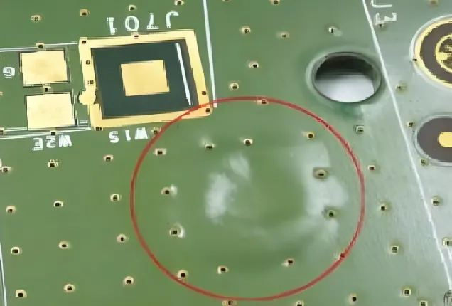
2. Bubbles in PCB Laminates: A Sign of Poor Bonding
Bubbles, or voids, are air pockets trapped within the PCB layers during the lamination process. These defects often appear as small blisters on the surface or between layers, compromising the board’s integrity.
Causes of Bubbles
- Moisture Contamination: If the prepreg material or copper foil contains moisture before lamination, it can vaporize under heat and pressure, forming bubbles.
- Insufficient Pressure: During lamination, inadequate pressure fails to remove air pockets, leading to trapped bubbles.
- Poor Material Storage: Storing materials in humid environments can introduce moisture, increasing the risk of bubble formation.
Impact on Manufacturing Yield
Bubbles weaken the bond between layers, reducing the PCB’s structural strength and potentially causing electrical failures. In severe cases, they can lead to a rejection rate of up to 10% in affected batches, as they often result in delamination during later stages of production or use.
Prevention Tips
- Store materials in a controlled, low-humidity environment to prevent moisture absorption.
- Optimize lamination parameters, ensuring adequate pressure (typically 200-300 psi) and temperature (around 180°C) to eliminate air pockets.
- Use vacuum lamination processes to remove air during manufacturing.
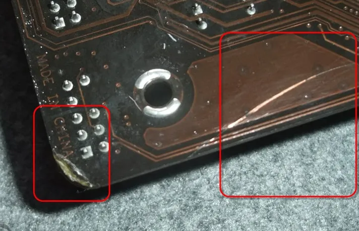
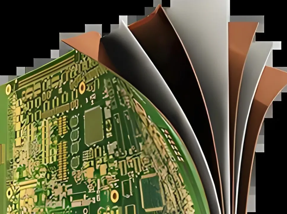
3. Delamination: When Layers Fall Apart
Delamination occurs when the layers of a PCB separate, often due to poor adhesion between the substrate and copper foil or between multiple layers. This defect appears as blisters or peeling and is a critical issue in PCB manufacturing.
Causes of Delamination
- Moisture Ingress: Humidity absorbed by the board can expand during soldering, causing layers to separate. For example, exposure to 85% relative humidity for 24 hours can significantly increase this risk.
- Thermal Shock: Rapid heating or cooling during reflow soldering can stress the adhesive bonds, leading to separation.
- Poor Material Compatibility: Using mismatched materials with different thermal properties can weaken bonds over time.
Impact on Manufacturing Yield
Delamination can cause complete board failure, as it disrupts electrical connections and structural integrity. In high-volume production, even a 5% delamination rate can result in thousands of defective units, severely impacting yield and profitability.
Prevention Tips
- Bake PCBs before soldering to remove absorbed moisture, typically at 120°C for 2-4 hours.
- Select materials with compatible thermal and mechanical properties to ensure strong bonding.
- Conduct adhesion tests during quality assurance to identify potential delamination risks early.
4. Wet Weaving: A Lesser-Known but Critical Defect
Wet weaving, also related to the fiber weave effect, refers to inconsistencies in the fiberglass weave used in PCB substrates. This defect occurs when the weave pattern is uneven or when resin does not fully penetrate the fiberglass during manufacturing, leaving gaps or weak spots.
Causes of Wet Weaving
- Inconsistent Resin Application: If the resin does not fully impregnate the fiberglass weave, it creates areas of uneven dielectric properties.
- Poor Material Quality: Low-grade fiberglass or prepreg materials may have inherent inconsistencies in weave density.
- High-Speed Signal Routing: For high-frequency designs, traces aligned over dense or sparse weave areas can experience signal integrity issues due to varying dielectric constants (typically ranging from 4.2 to 4.8).
Impact on Manufacturing Yield
Wet weaving can lead to signal skew in high-speed applications, where differential pairs experience timing delays (e.g., up to 10 ps/inch difference). This defect often results in boards failing electrical tests, contributing to a yield loss of around 8-12% in affected production runs.
Prevention Tips
- Use high-quality fiberglass materials with uniform weave patterns to ensure consistent dielectric properties.
- Rotate trace routing at a 45-degree angle relative to the weave to minimize the fiber weave effect on signal integrity.
- Work closely with material suppliers to ensure proper resin content and curing processes during manufacturing.
How to Improve Manufacturing Yield by Addressing PCB Defects
Preventing PCB defects like microcracks, bubbles, delamination, and wet weaving requires a combination of good design practices, high-quality materials, and strict process controls. Here are some overarching strategies to boost your manufacturing yield:
- Design for Manufacturability (DFM): Incorporate DFM principles early in the design phase to minimize stress points and ensure compatibility between materials. For example, avoid placing vias too close to board edges (maintain at least 10 mils clearance) to reduce mechanical stress.
- Quality Control and Testing: Use advanced inspection techniques like Automated Optical Inspection (AOI) and X-ray imaging to detect defects before they escalate. Testing a sample batch for thermal cycling (e.g., -40°C to 85°C for 100 cycles) can reveal potential weaknesses.
- Process Optimization: Fine-tune manufacturing parameters such as lamination pressure, curing time, and soldering temperatures to match the specific materials used. For instance, maintaining a reflow peak temperature below 260°C can reduce thermal stress.
- Supplier Collaboration: Partner with trusted material suppliers to ensure consistent quality and receive technical support for optimizing processes.
By implementing these strategies, manufacturers can reduce defect rates by up to 30%, significantly improving yield and reducing production costs.
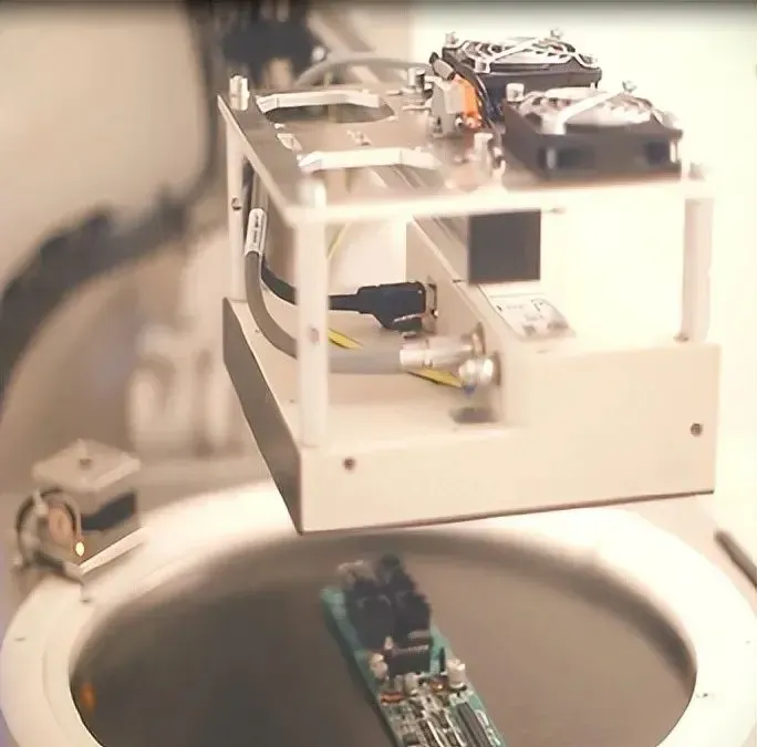
The Role of Technology in Detecting and Preventing PCB Defects
Modern technology plays a vital role in identifying and mitigating PCB defects. Tools like X-ray inspection systems can detect internal microcracks and bubbles with high precision, often identifying flaws as small as 0.1 mm. Similarly, automated testing equipment can measure signal integrity to catch wet weaving issues in high-speed designs, ensuring that impedance values remain within a tight tolerance (e.g., ±10% of 50 ohms for standard designs).
Additionally, simulation software allows engineers to predict thermal and mechanical stress points during the design phase, reducing the likelihood of delamination or microcracks. Investing in such technologies can increase upfront costs but pays off by improving yield and reducing long-term expenses.
Conclusion: Building Better PCBs with Fewer Defects
PCB defects such as microcracks, bubbles, delamination, and wet weaving are common challenges that can significantly affect manufacturing yield. By understanding their causes and impacts, and by implementing robust prevention strategies, manufacturers can produce high-quality boards that meet the demands of modern electronics. From using high-quality materials to leveraging advanced inspection technologies, every step counts in minimizing defects and maximizing yield.
At ALLPCB, we’re committed to supporting your journey toward flawless PCB production. With a focus on quality and innovation, we provide the tools and expertise needed to tackle these common defects head-on. Let’s work together to build reliable, high-performing PCBs that power the future of technology.


