ALLPCB


In the world of printed circuit board (PCB) fabrication, the solder mask plays a crucial role in ensuring both protection and performance. This thin layer of polymer, applied over the copper traces of a PCB, acts as a shield against environmental damage and prevents soldering errors. But why is it so important, and how does it impact the overall quality of a PCB? In this comprehensive guide, we’ll dive deep into the significance of solder mask, exploring its application process, materials, colors, registration accuracy, and its role in preventing solder bridging. Whether you’re an engineer, designer, or hobbyist, this blog will provide valuable insights to help you understand and optimize your PCB projects.
What Is a Solder Mask and Why Does It Matter?
A solder mask, often referred to as solder resist or solder stop, is a protective coating applied to the copper traces of a PCB. Its primary purpose is to insulate the copper, preventing oxidation and accidental short circuits during soldering. Without a solder mask, the exposed copper would be vulnerable to environmental factors like moisture and dust, leading to corrosion over time. Additionally, it helps avoid solder bridges—unintended connections between pads—during the assembly process, which can cause electrical failures.
Beyond protection, the solder mask enhances the performance and reliability of a PCB by ensuring precise soldering only where it’s needed. This layer is essential for mass production, especially in automated soldering techniques like reflow or wave soldering, where accuracy is critical. In short, the solder mask is a small but mighty component that directly impacts the durability and functionality of your electronic designs.
The Solder Mask Application Process: A Step-by-Step Overview
Understanding the solder mask application process is key to appreciating its role in PCB fabrication. This process involves several precise steps to ensure the mask is applied correctly and performs its protective duties. Here’s how it typically works:
- Cleaning the PCB Surface: Before applying the solder mask, the PCB surface is thoroughly cleaned to remove any contaminants like dust, grease, or oxidation. A clean surface ensures proper adhesion of the mask material.
- Coating Application: The solder mask material, usually a liquid photoimageable ink, is applied to the PCB. This can be done using methods like screen printing, curtain coating, or spray coating, depending on the type of mask and production scale.
- Pre-Baking: The coated PCB is pre-baked at a low temperature (around 75-85°C) to partially cure the mask and remove solvents. This step prepares the mask for the imaging process.
- Imaging and Exposure: Using a photomask or artwork, specific areas of the solder mask are exposed to UV light. The exposed areas harden, while unexposed areas remain soluble. This step defines where the mask will remain to protect the copper and where it will be removed to expose pads for soldering.
- Developing: The PCB is then washed with a developer solution to remove the unexposed solder mask material, revealing the copper pads and vias for soldering.
- Final Curing: The board undergoes a final curing process at a higher temperature (typically 120-150°C) to fully harden the solder mask, ensuring durability and resistance to heat and chemicals during assembly.
- Inspection: Finally, the PCB is inspected for defects like misalignment or incomplete coverage to ensure the solder mask meets quality standards.
This meticulous process ensures that the solder mask adheres properly and provides consistent protection across the board. Any errors in application can lead to issues like incomplete coverage or misalignment, which could compromise the PCB’s performance.
Solder Mask Materials Comparison: Choosing the Right Option
When it comes to selecting a solder mask, the material used can significantly affect the PCB’s performance and cost. Let’s break down a solder mask materials comparison to highlight the options available and their pros and cons:
- Epoxy Liquid Solder Mask: This is one of the most common and cost-effective options. Applied via screen printing, it offers good protection against oxidation and heat. However, it may lack precision for high-density designs due to its thicker application (typically 0.8-1.2 mils).
- Liquid Photoimageable (LPI) Solder Mask: LPI masks are widely used in modern PCB fabrication due to their precision. Applied as a thin layer (0.4-0.8 mils) and cured with UV light, they are ideal for fine-pitch components and high-density boards. They also offer excellent chemical resistance but can be more expensive than epoxy.
- Dry Film Solder Mask: This type is applied as a solid film and laminated onto the PCB. It provides uniform thickness and high resolution, making it suitable for complex designs. However, it’s less common due to higher costs and a more complex application process.
Choosing the right material depends on factors like the complexity of your PCB design, budget, and environmental conditions the board will face. For instance, LPI is often preferred for consumer electronics due to its balance of precision and durability, while epoxy might suffice for simpler, low-cost projects.
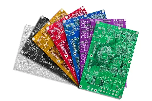
Solder Mask Colors and Their Uses: More Than Just Aesthetics
While green is the traditional and most recognized color for PCBs, solder mask colors and their uses go beyond mere appearance. Different colors are available, each with specific practical applications and benefits. Here’s a look at common options:
- Green: The standard choice due to its high contrast against copper traces and white silkscreen, making inspection and assembly easier. It’s also widely available and cost-effective, with good visibility under various lighting conditions.
- Red: Often used in prototyping or for aesthetic branding purposes. Red masks can make a PCB stand out, but they may reduce contrast with silkscreen text, making it harder to read.
- Blue: Popular in industrial and automotive applications, blue offers a modern look and decent contrast. It’s often chosen for branding or to differentiate between board revisions.
- Black: Used for high-end or visually appealing designs, black masks can hide traces for a sleek appearance. However, they absorb heat, which may not be ideal for high-temperature environments, and can make inspection challenging due to low contrast.
- White: Common in LED applications, white masks reflect light to enhance brightness. They’re less common for general use due to lower contrast and higher visibility of dirt or defects.
- Yellow and Other Custom Colors: These are less common but can be used for specific branding or niche applications. They often come at a higher cost due to limited availability.
The choice of color can impact not only the look of the PCB but also its functionality. For example, in high-frequency applications, heat dissipation is a concern, so darker colors like black might be avoided. Meanwhile, white might be ideal for LED boards where light reflection boosts performance by up to 10-15% in some cases.
Solder Mask Registration Accuracy: Precision Matters
Solder mask registration accuracy refers to how precisely the solder mask aligns with the copper pads and traces on the PCB. Poor registration can lead to exposed copper or covered pads, both of which can cause soldering issues or reliability problems. Achieving high accuracy is critical, especially for high-density interconnect (HDI) boards where pad sizes can be as small as 0.1 mm.
Modern fabrication processes use advanced imaging and alignment techniques to achieve registration accuracy within ±2 mils (0.002 inches). Factors that influence accuracy include:
- Artwork Quality: High-resolution photomasks ensure precise exposure of the solder mask.
- Equipment Calibration: State-of-the-art exposure and alignment machines reduce errors during application.
- Material Properties: Some solder mask materials, like LPI, offer better control over registration due to their thinner application.
Inaccurate registration can lead to defects like solder mask encroachment, where the mask partially covers pads, reducing the solderable area by 20-30% or more. This can weaken solder joints or cause assembly failures. Ensuring tight tolerances during design and fabrication is essential for maintaining performance, especially in fine-pitch components with spacing as tight as 0.5 mm.
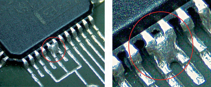
Preventing Solder Bridging: A Key Function of Solder Mask
One of the most critical roles of a solder mask is preventing solder bridging, an issue where excess solder forms an unintended connection between two closely spaced pads or traces. Solder bridges can create short circuits, leading to device malfunction or complete failure. With component pitches shrinking to 0.4 mm or less in modern designs, the risk of bridging has increased, making the solder mask more important than ever.
The solder mask works by creating a barrier between adjacent conductive areas, ensuring that solder only adheres to exposed pads during the reflow or wave soldering process. Its effectiveness depends on:
- Proper Coverage: The mask must fully cover areas between pads without gaps or pinholes, which could allow solder to flow unintentionally.
- Thickness Control: A mask that’s too thin (below 0.3 mils) may not provide adequate insulation, while one that’s too thick (above 1.5 mils) can interfere with component placement.
- Design Considerations: Designers must ensure adequate spacing between pads (at least 0.2 mm for fine-pitch components) and specify mask expansion (typically 2-4 mils larger than the pad) to prevent bridging.
By preventing solder bridging, the mask can reduce assembly defects by up to 90% in automated soldering processes, significantly improving yield rates and reliability. This is especially crucial in high-volume production where even a 1% defect rate can translate to thousands of failed units.
How Solder Mask Enhances Overall PCB Performance
Beyond protection, the solder mask contributes to the overall performance of a PCB in several ways. It improves dielectric properties, reducing signal interference in high-frequency applications where impedance control is critical (e.g., maintaining 50 ohms for RF signals). It also enhances thermal resistance, allowing PCBs to withstand soldering temperatures up to 260°C without degrading. Additionally, a well-applied solder mask can extend the lifespan of a PCB by protecting against environmental stressors, potentially increasing operational life by 5-10 years in harsh conditions.
For designers working on complex multilayer boards, the solder mask ensures consistent performance by maintaining insulation between layers, preventing issues like crosstalk or leakage currents. This reliability is vital for applications in industries like aerospace or medical devices, where failure is not an option.
Conclusion: Why Solder Mask Is Non-Negotiable in PCB Fabrication
The solder mask is far more than just a cosmetic layer on a PCB—it’s a fundamental component that ensures protection, precision, and performance. From shielding copper traces against oxidation to preventing solder bridging in tight-pitch designs, its role is indispensable. By understanding the solder mask application process, comparing materials, choosing the right color, ensuring registration accuracy, and leveraging its ability to prevent defects, you can significantly enhance the quality of your PCB projects.
At ALLPCB, we prioritize every detail of the fabrication process, including the application of high-quality solder masks tailored to your specific needs. Whether you’re working on a simple prototype or a complex multilayer design, incorporating the right solder mask strategy will safeguard your boards and optimize their performance for years to come.