 ALLPCB


For electrical engineers working on high-speed or RF designs, the choice of PCB plating can make or break signal integrity. PCB plating directly affects signal loss, impedance matching, and EMI shielding, among other critical factors. In this comprehensive guide, we’ll explore how PCB plating influences these aspects, diving into material properties, practical design tips, and real-world implications for RF circuits and beyond. Whether you're tackling signal loss or optimizing for high-frequency performance, understanding PCB plating is key to success.
Why PCB Plating Matters for Signal Integrity
Signal integrity refers to the quality of an electrical signal as it travels through a printed circuit board (PCB). Any distortion, loss, or interference can lead to data errors, reduced performance, or complete system failure. PCB plating—the thin layer of conductive material applied to the board's surface and vias—plays a significant role in maintaining signal integrity. It impacts how signals propagate, how much loss occurs, and how well the board shields against electromagnetic interference (EMI).
For engineers designing high-speed digital circuits or RF systems, plating choices can affect critical parameters like impedance, crosstalk, and signal attenuation. Let’s break down the specific ways PCB plating influences these factors, focusing on long-tail concerns like PCB plating and signal loss, PCB plating for RF circuits, and more.
What Is PCB Plating?
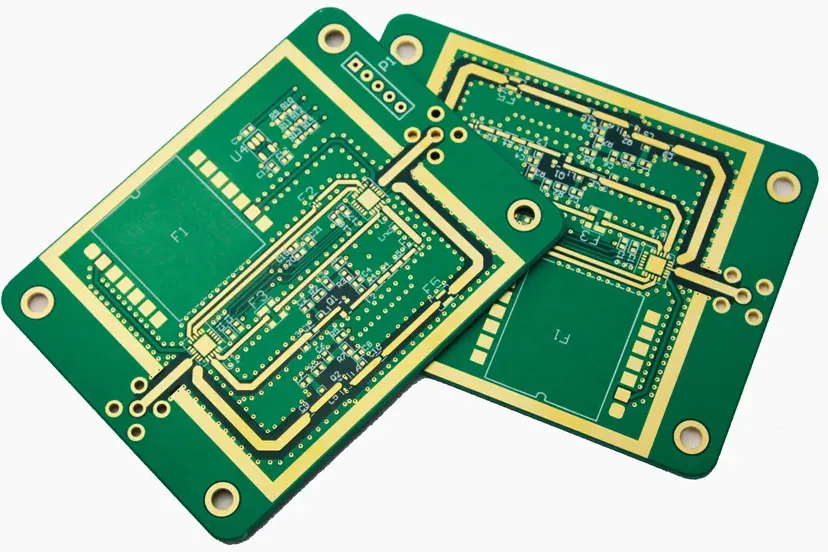
PCB plating is the process of depositing a conductive material, typically copper, gold, or silver, onto the surface of a PCB and inside its vias. This layer ensures electrical connectivity, protects against corrosion, and enhances durability. Common plating types include:
- Electroless Nickel Immersion Gold (ENIG): A popular choice for its corrosion resistance and flat surface, ideal for fine-pitch components.
- Immersion Silver: Offers excellent conductivity but is prone to tarnishing.
- Hard Gold: Durable and used for connectors, though less common for signal paths due to cost.
- Immersion Tin: Cost-effective but less durable over time.
Each plating type has unique electrical and mechanical properties that influence signal behavior. Let’s dive deeper into these effects.
PCB Plating and Signal Loss: A Critical Connection
Signal loss, or attenuation, occurs when a signal weakens as it travels through a PCB trace. For high-speed designs operating at frequencies above 1 GHz, even small losses can degrade performance. PCB plating contributes to signal loss through two primary mechanisms: conductor loss and skin effect.
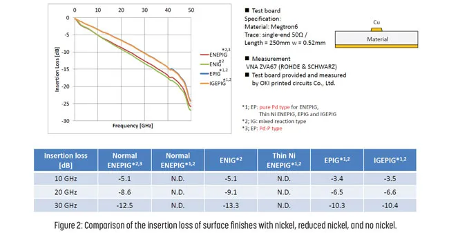
Conductor Loss: The resistivity of the plating material affects how much energy is lost as heat. For instance, copper, often used as the base conductor, has a resistivity of about 1.68 x 10^-8 Ω·m. However, surface plating like ENIG introduces a thin layer of nickel (with higher resistivity around 6.84 x 10^-8 Ω·m), which can increase conductor loss slightly.
Skin Effect: At high frequencies, current flows primarily on the surface of a conductor. If the plating material has poor conductivity or roughness, it exacerbates signal loss. Immersion Silver, with its high conductivity, performs better than ENIG in this regard for RF applications.
For engineers working on designs where PCB plating and signal loss are concerns, choosing a plating with minimal resistivity and smooth surface finish is critical. Studies show that rough plating surfaces can increase signal loss by up to 20% at frequencies above 5 GHz due to increased skin effect losses.
Practical Tip: When designing for minimal signal loss, consider specifying a low-roughness copper foil and pairing it with Immersion Silver plating for high-frequency traces. Always consult your PCB manufacturer about surface finish options and their impact on loss.
PCB Plating for RF Circuits: Optimizing High-Frequency Performance
Radio frequency (RF) circuits operate at frequencies where signal integrity challenges are amplified. For RF designs, PCB plating for RF circuits must minimize loss, ensure consistent impedance, and reduce parasitic effects. The choice of plating can significantly impact performance in the following ways:
Signal Attenuation: As discussed, high-frequency signals are prone to attenuation due to skin effect. Plating materials like Immersion Silver or bare copper with a smooth finish are often preferred for RF traces to reduce loss.
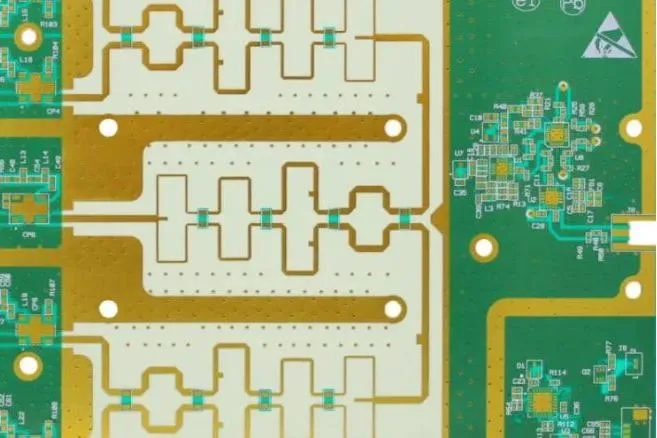
Parasitic Capacitance and Inductance: Plating inside vias can introduce parasitic effects if not carefully controlled. For instance, thick nickel layers in ENIG plating can increase parasitic capacitance, affecting RF signal timing and phase.
Dielectric Interaction: The plating material interacts with the PCB substrate’s dielectric properties. A mismatch can lead to signal reflection and loss. Engineers often pair RF-friendly plating with low-loss dielectrics like Rogers or PTFE materials for optimal results.
Real-World Example: In a 5G antenna design project, engineers found that switching from ENIG to Immersion Silver plating reduced signal attenuation by 15% at 28 GHz, significantly improving the antenna’s efficiency. This highlights the importance of tailoring plating choices to specific RF requirements.
Practical Tip: For RF circuits, prioritize plating materials with high conductivity and minimal thickness to reduce parasitic effects. Work closely with your PCB fabricator to ensure consistent plating thickness across critical areas.
PCB Plating Material Properties: What Engineers Need to Know
The material properties of PCB plating directly influence electrical performance. When evaluating PCB plating material properties, consider the following factors:
Conductivity: Higher conductivity reduces resistive losses. Silver offers the best conductivity (6.3 x 10^7 S/m), followed by copper (5.96 x 10^7 S/m). Nickel, often used in ENIG, lags at 1.46 x 10^7 S/m, making it less ideal for high-speed signals.
Corrosion Resistance: Plating must withstand environmental factors. ENIG excels here due to its gold top layer, protecting underlying copper from oxidation. Immersion Silver, while conductive, tarnishes over time, potentially increasing contact resistance.
Surface Roughness: Rough surfaces scatter high-frequency signals, increasing loss. Modern plating processes aim for smoothness, often measured as Ra (average roughness) in micrometers. A Ra value below 0.5 μm is ideal for high-frequency designs.
Thermal Stability: Plating must endure soldering temperatures without degrading. Hard Gold withstands thermal stress better than Immersion Tin, which can form whiskers under heat.
Understanding these properties helps engineers select the right plating for their application. For instance, a high-speed digital board might prioritize conductivity with Immersion Silver, while a rugged industrial design might opt for ENIG’s durability.
PCB Plating Effect on Impedance Matching: Precision Matters
Impedance matching ensures maximum power transfer and minimizes signal reflections in a circuit. For high-speed and RF designs, maintaining a consistent characteristic impedance (often 50 ohms for RF or 100 ohms differential for high-speed digital) is critical. The PCB plating effect on impedance matching comes into play through several mechanisms:
Trace Geometry: Plating thickness affects the effective width and height of traces, altering impedance. A typical plating thickness of 1-2 μm might seem negligible, but at frequencies above 10 GHz, even small variations can shift impedance by 5-10%.
Dielectric Constant Influence: Plating inside vias and on pads interacts with the PCB’s dielectric material, potentially causing impedance discontinuities. For example, nickel in ENIG has a different permittivity than copper, introducing slight mismatches.
Vias and Transitions: Plated vias can create impedance mismatches if the plating is uneven or too thick. This is especially problematic in multi-layer boards where signals transition between layers.
Practical Tip: Use simulation tools like Altium or Cadence to model the impact of plating on impedance. Specify tight tolerances for plating thickness (e.g., ±0.5 μm) when working on impedance-controlled designs. Additionally, consider controlled-depth drilling for vias to minimize plating inconsistencies.
Real-World Example: During a 10 Gbps Ethernet board design, engineers noticed a 7% impedance mismatch at via transitions due to uneven ENIG plating. Switching to a thinner Immersion Silver layer and optimizing via design resolved the issue, reducing reflections.
PCB Plating and EMI Shielding: Protecting Your Design
Electromagnetic interference (EMI) can disrupt signal integrity by introducing noise into a circuit. Effective PCB plating and EMI shielding are essential for maintaining performance, especially in dense, high-speed designs. Plating contributes to EMI shielding in the following ways:
Ground Planes: A solid, well-plated ground plane acts as a shield, absorbing and redirecting stray electromagnetic fields. ENIG or Hard Gold plating on ground planes ensures low resistance and durability.
Vias and Stitching: Plated through-hole vias, often filled with conductive material, create a “cage” effect around sensitive traces, reducing EMI. Consistent plating quality in vias is crucial for effective shielding.
Surface Conductivity: High-conductivity plating like Immersion Silver enhances the effectiveness of shielding layers by minimizing resistive losses in the shield.
Practical Tip: For EMI-sensitive designs, use a multi-layer PCB with dedicated ground and power planes. Ensure that plating on these planes is uniform and specify a high-conductivity finish. Additionally, place via stitching around high-speed traces to form a Faraday cage effect, reducing EMI by up to 30% in some cases.
Practical Design Considerations for Engineers
Now that we’ve covered the technical impacts of PCB plating on signal integrity, let’s summarize actionable steps for electrical engineers:
- Match Plating to Application: Choose plating based on frequency, environmental conditions, and budget. Use Immersion Silver for high-frequency RF circuits and ENIG for durability in harsh environments.
- Collaborate with Fabricators: Work closely with your PCB manufacturer to ensure consistent plating thickness and surface roughness. Request test coupons to verify impedance and loss characteristics.
- Simulate and Test: Use EDA tools to simulate signal behavior with different plating options. Validate designs with time-domain reflectometry (TDR) to measure impedance and loss after fabrication.
- Prioritize Signal Paths: Apply high-conductivity plating selectively to critical signal traces if cost is a concern, reserving durable finishes like Hard Gold for connectors and pads.
Challenges and Trade-Offs in PCB Plating Choices
No plating option is perfect. Engineers often face trade-offs between cost, performance, and reliability. For instance:
- ENIG offers excellent corrosion resistance but introduces higher conductor loss due to nickel.
- Immersion Silver provides superior conductivity but tarnishes over time, risking long-term reliability.
- Hard Gold is durable for connectors but expensive for large areas.
Balancing these trade-offs requires a clear understanding of project priorities. For a low-cost consumer device, Immersion Tin might suffice despite its limitations. For a mission-critical RF system, the added cost of Immersion Silver or custom finishes may be justified.
Conclusion: Making Informed Decisions on PCB Plating
PCB plating is more than a surface-level concern—it’s a fundamental factor in achieving robust signal integrity. From minimizing signal loss to optimizing impedance matching and enhancing EMI shielding, the right plating choice can elevate your design’s performance. By understanding the nuances of PCB plating and signal loss, PCB plating for RF circuits, PCB plating material properties, PCB plating effect on impedance matching, and PCB plating and EMI shielding, electrical engineers can make informed decisions tailored to their specific needs.
Remember, collaboration with your PCB fabricator and rigorous simulation are key to success. Whether you’re designing a high-speed digital board or a cutting-edge RF system, don’t overlook the impact of plating. Take the time to evaluate options, test prototypes, and refine your approach. Your signals—and your end users—will thank you.


