 ALLPCB


If you're dealing with unexpected short circuits on your printed circuit board (PCB), solder bridging might be the culprit. A solder bridge is an unintended connection between two or more conductive points on a PCB, often caused by excess solder. This can lead to malfunctioning circuits and costly rework. In this comprehensive guide, we'll break down what solder bridging is, how to identify and repair it using techniques like solder wick vs solder sucker, and share actionable tips for preventing solder bridges in SMT (Surface Mount Technology) assembly. We'll also cover critical aspects like solder paste volume bridging and PCB design spacing for solder bridge prevention. Let's dive into solving this common electronics issue with practical, step-by-step advice.
What Is Solder Bridging and Why Does It Happen?
Solder bridging occurs when excess solder forms an unintended connection between two adjacent pads, pins, or traces on a PCB. This creates a short circuit, which can disrupt the functionality of the board by allowing current to flow where it shouldn't. These bridges are particularly common in high-density PCB designs or during SMT assembly, where components and pads are placed very close together.
Common causes of solder bridging include:
- Excess Solder Application: Applying too much solder during manual soldering or using excessive solder paste in automated processes.
- Improper Component Placement: Misaligned components can cause solder to flow between unintended areas.
- Inadequate Spacing: When pads or traces are too close together, solder can easily bridge the gap.
- Poor Stencil Design: In SMT, a poorly designed stencil can deposit uneven amounts of solder paste, leading to bridging.
- Thermal Issues: Incorrect reflow profiles during soldering can cause solder to spread unpredictably.
Understanding these causes is the first step to prevention and effective repair. Solder bridging not only affects the performance of a single board but can also lead to batch failures in mass production if not addressed.
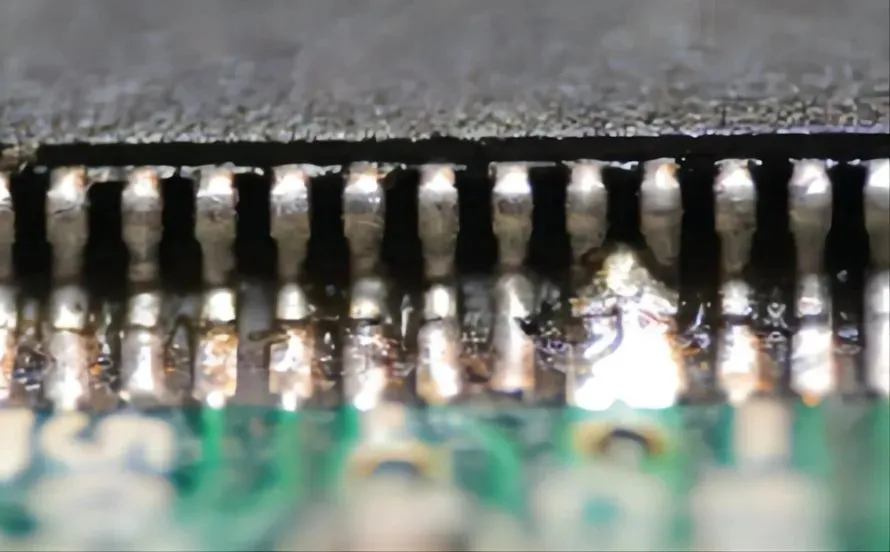
How to Identify Solder Bridging on Your PCB
Spotting a solder bridge can save you hours of troubleshooting. Here are the key signs to look for:
- Visual Inspection: Use a magnifying glass or microscope to check for visible solder connections between adjacent pads or pins. Bridges often appear as small blobs or lines of solder where there should be separation.
- Electrical Testing: If your circuit isn't working as expected, use a multimeter set to continuity mode. Test between adjacent pins or pads; a beep or low resistance reading (close to 0 ohms) indicates a short circuit caused by a bridge.
- Functional Failure: If components are overheating or the board fails to operate, a solder bridge could be redirecting current improperly.
Identifying solder bridges early, especially during the prototyping phase, can prevent larger issues down the line. For high-density boards, automated optical inspection (AOI) systems can help detect bridges that are too small to see with the naked eye.
Related Reading: Solder Bridges: The Silent Killer of PCB Performance
Solder Bridge Repair: Step-by-Step Techniques
Once you've identified a solder bridge, the next step is to remove it safely without damaging the PCB or components. Below are two popular methods for solder bridge repair: using solder wick and using a solder sucker. We'll compare solder wick vs solder sucker to help you choose the right tool for the job.
Method 1: Using Solder Wick (Desoldering Braid)
Solder wick, also known as desoldering braid, is a braided copper wire coated with flux. It absorbs excess solder through capillary action when heated. Here's how to use it:
- Heat your soldering iron to around 300°C (572°F), depending on the solder type (lead-free solder may require higher temperatures).
- Place the solder wick over the solder bridge.
- Press the heated soldering iron tip onto the wick over the bridge. The heat will transfer through the wick, melting the solder, which gets absorbed into the braid.
- Remove the wick and iron together once the solder is absorbed. Trim off the used portion of the wick.
- Inspect the area to ensure the bridge is gone. If necessary, repeat the process.
Pros of Solder Wick: It's precise and ideal for small, delicate areas on a PCB. It works well for SMT components where space is tight.
Cons: It can be time-consuming for large amounts of solder and may leave residue if not cleaned properly.
Method 2: Using a Solder Sucker (Desoldering Pump)
A solder sucker is a manual or electric pump that creates suction to remove molten solder. Follow these steps:
- Heat the soldering iron to the appropriate temperature (around 300°C or 572°F).
- Melt the solder bridge by placing the iron tip on it.
- Quickly position the solder sucker's nozzle over the molten solder and press the release button to suck it up.
- Repeat if necessary and clean the area with isopropyl alcohol to remove flux residue.
Pros of Solder Sucker: It's faster for larger solder bridges and can handle bigger solder volumes.
Cons: It requires more skill to avoid damaging delicate components, and the suction might not work well in tight spaces.
Solder Wick vs Solder Sucker: Which Is Better?
Choosing between solder wick vs solder sucker depends on the situation:
- Use solder wick for precision work, especially on small SMT components or tight spaces.
- Use a solder sucker for larger bridges or through-hole components where speed is more important than precision.
Both tools are affordable and widely available, so having them in your toolkit is a smart move for any electronics enthusiast or professional.
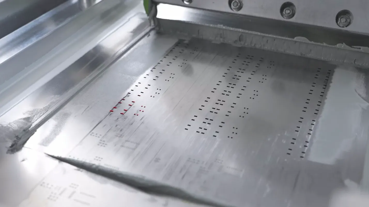
Preventing Solder Bridges in SMT Assembly
Preventing solder bridges in SMT is critical for high-quality PCB assembly, especially since surface mount components are small and densely packed. Here are proven strategies to avoid bridging during SMT soldering:
1. Optimize Solder Paste Application
Solder paste volume bridging is a common issue in SMT. Too much solder paste can overflow during reflow, creating bridges. To prevent this:
- Use a stencil with appropriately sized apertures. For fine-pitch components (e.g., 0.5mm pitch), reduce aperture size by 10-20% to control paste volume.
- Ensure the stencil thickness is suitable—typically 0.1mm to 0.15mm for most SMT applications.
- Regularly clean the stencil to avoid paste buildup, which can lead to uneven deposits.
2. Control Reflow Profiles
The reflow soldering process must be carefully controlled. A proper temperature profile ensures that solder paste melts and flows correctly without spreading to adjacent pads. Key parameters include:
- Preheat Zone: Gradually heat to 150-180°C over 60-90 seconds to activate flux and prevent thermal shock.
- Reflow Zone: Peak at 235-250°C for 20-40 seconds to melt solder without excessive spreading.
- Cooling Zone: Cool at a rate of 2-4°C per second to solidify solder evenly.
Monitor and adjust the profile based on your specific solder paste specifications to minimize bridging risks.
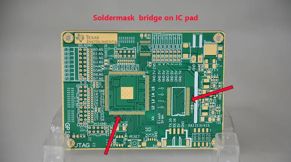
3. Use Solder Mask Correctly
A well-designed solder mask layer prevents solder from flowing to unwanted areas. Ensure the mask covers areas between closely spaced pads, leaving only the intended soldering areas exposed.
PCB Design Spacing for Solder Bridge Prevention
One of the most effective ways to avoid solder bridging is through smart PCB layout design. PCB design spacing for solder bridge prevention involves creating enough separation between conductive elements to minimize the risk of unintended connections. Here are key design tips:
1. Increase Pad-to-Pad Spacing
For fine-pitch components, maintain a minimum spacing of at least 0.2mm between pads. For larger components, aim for 0.3mm or more. This reduces the chance of solder flowing between pads during reflow.
2. Optimize Trace Routing
Avoid routing traces too close to pads or other traces. A minimum clearance of 0.15mm to 0.25mm between traces and pads helps prevent accidental bridging during soldering.
3. Use Teardrop Pads
Teardrop-shaped pads (where the pad narrows as it connects to a trace) can help control solder flow and reduce the likelihood of bridges forming at pad-to-trace junctions.
4. Incorporate Solder Mask Between Pads
For high-density designs, ensure solder mask webs (thin strips of mask material) are placed between closely spaced pads. A mask web of at least 0.1mm width can act as a barrier to prevent solder from spreading.
By prioritizing spacing and mask design, you can significantly lower the risk of solder bridging right from the design stage. Many modern design software tools allow you to set design rule checks (DRC) to enforce minimum spacing requirements automatically.
Related Reaing: Design for Excellence: Eliminating Solder Bridges in High Density PCBs
Additional Tips for Solder Bridge Prevention
Beyond SMT techniques and PCB design, here are more general practices to keep solder bridging at bay:
- Manual Soldering Care: When soldering by hand, use the correct tip size (e.g., a 1mm tip for fine-pitch work) and apply only the necessary amount of solder. Avoid dragging the iron across pads.
- Component Placement Accuracy: Ensure components are aligned correctly before soldering. Misalignment can cause solder to flow between unintended areas.
- Clean Boards: Remove dust, debris, or old flux residue from the PCB before soldering. Contaminants can cause solder to behave unpredictably.
- Regular Inspections: After soldering, inspect every board under magnification or with AOI to catch bridges early.
Conclusion: Master Solder Bridging for Reliable PCBs
Solder bridging is a common challenge in PCB assembly, but with the right knowledge and tools, it’s entirely manageable. By understanding how to identify and repair bridges using methods like solder wick or a solder sucker, you can fix issues quickly and efficiently. More importantly, focusing on prevention—whether through optimizing solder paste volume bridging in SMT, ensuring proper PCB design spacing for solder bridge prevention, or refining soldering techniques—can save time and resources in the long run.
Whether you're a hobbyist or a professional engineer, incorporating these strategies into your workflow will lead to more reliable and high-performing circuit boards. Keep your designs clean, your soldering precise, and your inspections thorough, and solder bridging will no longer be a mystery but a solvable challenge.


