 ALLPCB


Designing a circuit board for 3D printing is an exciting and innovative way to create custom electronics at home. By combining 3D printing technology with circuit design, you can prototype low-cost PCBs (Printed Circuit Boards) for your DIY projects without relying on expensive manufacturing services. This guide will walk you through the process of designing a circuit board tailored for 3D printing, offering practical steps and tips to help you succeed in your DIY design journey.
Whether you’re a hobbyist or a budding engineer, this blog post will break down everything you need to know about 3D printing circuit design. From the basics of PCB layout to printing techniques and material choices, we’ve got you covered. Let’s dive into the world of low-cost PCB creation at home!
What Is 3D Printing for Circuit Boards?
3D printing for circuit boards involves using a 3D printer to create the physical structure of a PCB or to assist in the fabrication process. Unlike traditional PCB manufacturing, which often requires complex chemical etching and professional equipment, 3D printing offers a more accessible approach for DIY enthusiasts. This method allows you to print the board’s substrate (the base layer) or create templates for conductive traces, making it a low-cost solution for prototyping at home.
The primary advantage of 3D printing in circuit design is the ability to iterate quickly. You can test different designs, make adjustments, and print new versions within hours. This is especially useful for small-scale projects or experimental circuits where sending designs to a manufacturer might not be cost-effective.
Why Choose 3D Printing for Circuit Design?
Opting for 3D printing in circuit design comes with several benefits, especially for those working on DIY projects or looking for low-cost PCB solutions at home. Here are some reasons to consider this approach:
- Cost-Effective: Traditional PCB manufacturing can be expensive for small runs. With 3D printing, you can create prototypes for a fraction of the cost using affordable materials like PLA or ABS filament.
- Speed: Printing a circuit board at home takes hours, not days or weeks, compared to ordering from a manufacturer.
- Customization: 3D printing allows you to experiment with unique shapes and structures that might not be feasible with standard PCB fabrication methods.
- Learning Opportunity: Designing and printing your own circuit boards is a hands-on way to understand electronics and manufacturing processes.
Steps to Design a Circuit Board for 3D Printing
Designing a circuit board for 3D printing involves a combination of electronic design and 3D modeling skills. Below, we’ll outline the key steps to guide you through the process, ensuring your DIY design is both functional and practical for low-cost PCB creation at home.
Step 1: Plan Your Circuit Design
Before you start printing, you need a clear idea of the circuit you want to build. Begin by sketching the schematic of your circuit, which is a diagram showing how components like resistors, capacitors, and microcontrollers connect. This schematic will serve as the blueprint for your PCB layout.
Use free or open-source software tools to create your schematic. These tools often have libraries of components with predefined electrical properties, making it easier to design accurate circuits. Ensure your design accounts for critical factors like voltage requirements (e.g., 5V for most microcontrollers) and current limits to avoid damaging components.
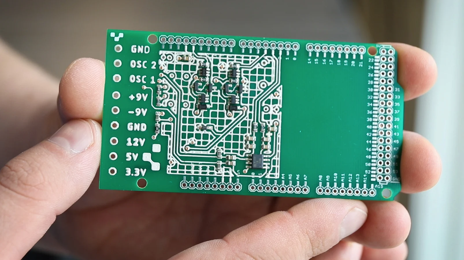
Step 2: Create the PCB Layout
Once your schematic is ready, translate it into a PCB layout. This layout determines where components will be placed on the board and how the conductive traces (the paths for electrical signals) will connect them. Pay attention to trace width, as it affects the current-carrying capacity. For example, a trace width of 0.254mm can typically handle up to 0.5A of current for low-power applications.
Keep signal integrity in mind by minimizing trace lengths for high-speed signals (e.g., above 1 MHz) to reduce impedance, which can interfere with performance. Also, ensure proper spacing between traces to prevent short circuits— a minimum of 0.2mm is often recommended for DIY designs.
Step 3: Design the 3D Model for Printing
After finalizing the PCB layout, it’s time to prepare the 3D model of the board’s substrate. Use 3D modeling software to create a base layer that matches the dimensions of your PCB layout. Common materials for printing include PLA or ABS, but for better heat resistance near components, consider PETG or nylon.
In your 3D model, include channels or grooves where conductive traces will go. These grooves can later be filled with conductive materials like silver ink or copper wire. Ensure the board thickness is at least 1.6mm (a standard PCB thickness) to provide structural stability.
Step 4: Choose the Right Printing Method
There are two main approaches to 3D printing circuit boards: printing the entire board with conductive materials or printing a non-conductive base and adding conductive traces afterward. Here’s a breakdown of both methods for your DIY design:
- Fully Conductive Printing: Some advanced 3D printers support conductive filaments made from carbon or graphene. These materials can print traces directly, but they often have higher resistance (e.g., 10 ohms per cm) compared to copper, making them unsuitable for high-current applications.
- Hybrid Approach: Print a non-conductive base using standard filament and manually add conductive traces using conductive paint or thin copper strips. This method is more accessible for low-cost PCB creation at home and offers better conductivity.
Step 5: Print the Circuit Board Base
Load your 3D model into your printer’s slicing software and adjust settings for optimal results. Use a high infill percentage (around 80-100%) to ensure the board is sturdy. Set the layer height to 0.2mm or lower for smoother surfaces, especially if you’re creating grooves for traces.
After printing, inspect the board for defects like warping or uneven surfaces. Sand down rough areas if needed to ensure components sit flat during assembly.
Step 6: Add Conductive Traces
If you’ve used the hybrid approach, it’s time to add the conductive traces to your printed board. Apply conductive paint or ink into the grooves using a fine brush or syringe for precision. Alternatively, lay thin copper wires or tape along the paths and secure them with adhesive.
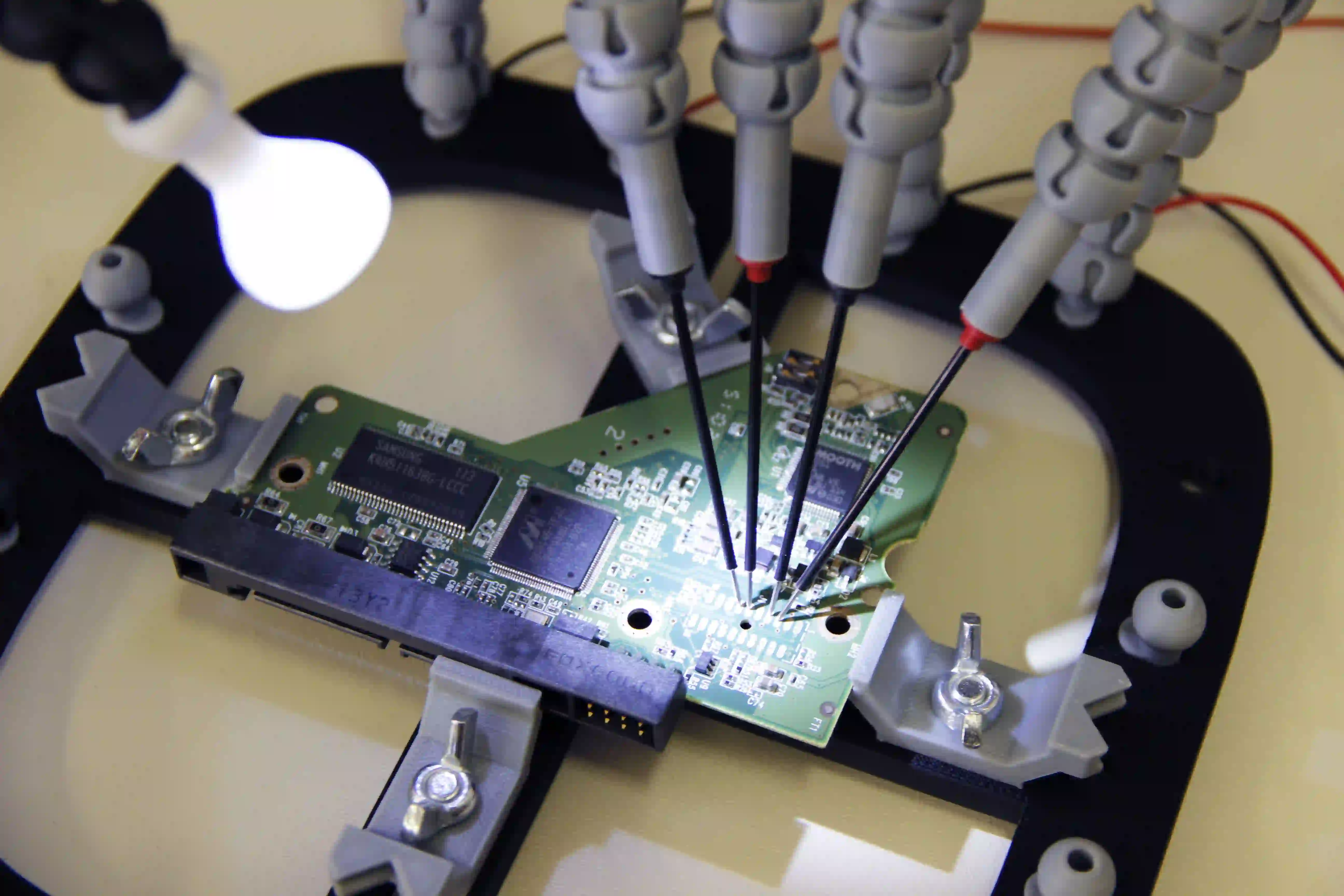
Test the conductivity of each trace with a multimeter to ensure there are no breaks. A typical copper trace should show near-zero resistance (less than 0.1 ohms over a short distance). If resistance is high, reapply the conductive material or check for gaps.
Step 7: Assemble and Test the Circuit
Place your components onto the board, aligning them with the designated spots from your layout. Solder them in place if necessary, ensuring clean connections. Double-check polarity for components like LEDs and capacitors to avoid damage.
Power up the circuit and test its functionality. Use a multimeter to measure voltages at key points (e.g., 3.3V or 5V at microcontroller pins) to confirm everything operates within expected ranges. If issues arise, trace back through your design to identify errors in the layout or connections.
Materials and Tools for 3D Printing Circuit Boards
To successfully design and print a circuit board at home, you’ll need the right materials and tools. Here’s a list tailored for low-cost PCB creation and DIY design:
- 3D Printer: A basic FDM (Fused Deposition Modeling) printer works well for most projects. Ensure it has a build volume large enough for your board size.
- Filament: PLA or ABS for basic boards; PETG for better heat resistance near soldered components.
- Conductive Materials: Conductive paint, silver ink, or copper tape for traces.
- Design Software: Free tools for schematic and PCB layout design, plus 3D modeling software for creating the board structure.
- Basic Electronics Tools: Soldering iron, multimeter, and wire cutters for assembly and testing.
Challenges and Tips for 3D Printed Circuit Boards
While 3D printing offers a fantastic way to create low-cost PCBs at home, it’s not without challenges. Here are some common issues and tips to overcome them in your DIY design process:
- Conductivity Issues: Conductive filaments often have higher resistance than copper. Stick to the hybrid approach for better performance in high-current circuits.
- Heat Resistance: Standard 3D printing materials like PLA can deform under heat from soldering. Use PETG or apply low-temperature soldering techniques.
- Precision: Ensure your printer is calibrated for accurate dimensions, as small errors can misalign traces and components. Aim for a tolerance of ±0.1mm.
- Durability: 3D printed boards may not be as robust as professionally made PCBs. Handle them carefully and avoid high-stress applications.
Benefits of Partnering with Professionals for Final Production
While 3D printing is excellent for prototyping and small-scale DIY projects, scaling up or creating complex designs often requires professional manufacturing. Partnering with a reliable service for final production ensures high-quality boards with precise trace widths (down to 0.1mm) and multi-layer capabilities that are difficult to achieve at home. This approach saves time and guarantees reliability for critical applications.
Conclusion: Start Your 3D Printing Circuit Design Journey Today
Designing a circuit board for 3D printing opens up a world of possibilities for hobbyists and engineers alike. With the right tools, materials, and steps, you can create low-cost PCBs at home, perfect for prototyping and learning. From planning your circuit to printing and testing, this guide has covered the essentials of DIY design using 3D printing technology.
Embrace the flexibility and creativity that 3D printing offers in circuit design. Start small, experiment with different layouts, and refine your skills over time. With each project, you’ll gain a deeper understanding of electronics and manufacturing, paving the way for more ambitious creations. Dive into the exciting intersection of 3D printing and circuit design today, and bring your ideas to life!


