ALLPCB


If you're a hobbyist diving into the world of electronics, understanding PCB form factor is a crucial first step in creating functional and efficient designs. But what exactly is a PCB form factor, and why does it matter for your DIY PCB design projects? In simple terms, a PCB form factor refers to the physical shape, size, and layout specifications of a printed circuit board (PCB) that determine how it fits into a device or system. This guide is tailored for beginners, walking you through the essentials of PCB form factor, layout, and design, with practical tips for home PCB fabrication, simple PCB layouts, and using easy PCB software for basic electronics projects.
Whether you're building a small gadget or experimenting with circuits at home, this comprehensive guide will help you master the basics of PCB design. Let’s explore the key concepts, tools, and steps to create your own boards with confidence.
What Is a PCB Form Factor and Why Does It Matter?
A PCB form factor defines the physical dimensions and mounting specifications of a circuit board. It ensures that your PCB fits into its intended enclosure or device and aligns with connectors, screws, and other components. For hobbyists working on DIY PCB design, choosing the right form factor is essential to avoid compatibility issues and ensure your project functions as intended.
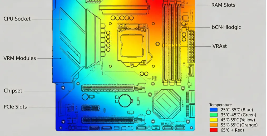
Common form factors include standards like ATX (used in desktop computers), Micro-ATX, and smaller formats like those for single-board computers (e.g., Raspberry Pi). However, as a beginner, you might not always need to follow strict industry standards. For basic electronics projects, you can often create custom form factors tailored to your specific needs, as long as you account for component placement and enclosure constraints.
Understanding form factor is especially important for home PCB fabrication. A poorly planned form factor can lead to wasted materials, mismatched components, or boards that don’t fit in your project box. By starting with a clear idea of your board’s size and shape, you’ll save time and effort in the long run.
Key Considerations for PCB Form Factor in DIY Design
When planning your PCB form factor for a DIY project, there are several factors to keep in mind. These will help you create simple PCB layouts that are both functional and easy to fabricate at home.
1. Size and Shape of the Board
The size of your PCB should match the enclosure or device it will be housed in. Measure the available space carefully before designing. For example, if you’re building a small wearable device, your board might need to be less than 2 inches by 2 inches. On the other hand, a larger project like a home automation controller might allow for a board size of 4 inches by 6 inches or more.
The shape is equally important. Most PCBs are rectangular for simplicity, but you can experiment with circular or irregular shapes if your project demands it. Just remember that non-standard shapes can complicate home PCB fabrication due to cutting and drilling challenges.
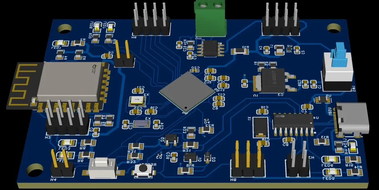
2. Component Placement and Mounting Holes
Your form factor must accommodate all components, such as resistors, capacitors, microcontrollers, and connectors. Plan their placement to minimize signal interference and heat buildup. For instance, keep high-power components away from sensitive analog circuits to avoid noise issues. A general rule of thumb is to maintain at least 0.1 inches (2.54 mm) of clearance between components for easy soldering and heat dissipation.
Don’t forget to include mounting holes in your design. These holes, typically 3-5 mm in diameter, allow you to secure the PCB inside an enclosure using screws. Place them near the corners of the board for stability.
3. Connector and Port Alignment
If your project includes external connections like USB ports, power jacks, or sensor inputs, ensure they align with openings in your enclosure. Misaligned connectors can make your board unusable. During the design phase, double-check the dimensions of these components and their placement on the PCB edge.
Steps to Design a PCB Form Factor for Beginners
Designing a PCB form factor might seem intimidating, but with the right approach and tools, it’s manageable even for hobbyists. Follow these steps to create a functional design for your basic electronics projects.
Step 1: Define Your Project Requirements
Start by listing the components you’ll need on your PCB. For a simple project like an LED blinker, you might only need a microcontroller, a few resistors, LEDs, and a power source. For more complex projects, such as a home automation sensor, you might include Wi-Fi modules, relays, and multiple sensors. Knowing your components helps determine the board size and shape.
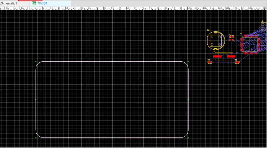
Step 2: Sketch a Rough Layout
Before diving into software, grab a piece of paper and sketch a rough layout of your PCB. Place major components first, followed by smaller ones. This sketch will serve as a blueprint when you move to digital design tools. Keep traces (the conductive paths connecting components) as short as possible to reduce signal loss. For example, a trace longer than 10 inches for a high-speed signal (above 50 MHz) can introduce delays or noise.
Step 3: Choose Easy PCB Software for Design
For beginners, using user-friendly PCB design software is a game-changer. Many free or low-cost tools are available that simplify the design process. Look for software with drag-and-drop interfaces, built-in component libraries, and tutorials. These tools often include features to set board dimensions and create custom form factors easily.
Start by setting your board outline in the software based on your sketch. Then, place components and route traces. Most programs will also let you run design rule checks (DRC) to catch errors like overlapping traces or insufficient clearances. A common clearance standard for hobbyist designs is 0.008 inches (0.2 mm) between traces to prevent short circuits.
Step 4: Test and Refine Your Design
Once your design is complete, export a preview of the board and check for errors. Ensure that all components fit within the form factor and that traces don’t cross unnecessarily. If possible, print a 1:1 scale version of your design on paper and place physical components on it to verify spacing. Refine the layout as needed before moving to fabrication.
Home PCB Fabrication: Turning Designs into Reality
After finalizing your PCB form factor and layout, the next step is fabrication. Home PCB fabrication is a rewarding process for hobbyists, allowing you to create custom boards without relying on external services. Here’s how to get started with simple PCB layouts.
1. Gather Materials and Tools
You’ll need a few basic supplies for home PCB fabrication:
- Copper-clad board (single or double-sided, depending on your design)
- Ferric chloride or another etchant for removing unwanted copper
- Laser printer and glossy paper for transferring your design
- Drill bits for creating holes (0.8-1.2 mm for most components)
- Soldering iron and solder for assembling components
These materials are affordable and widely available online or at local electronics stores.
2. Transfer Your Design to the Board
Print your PCB layout using a laser printer on glossy paper. Place the printed design face-down on the copper-clad board and use an iron to transfer the toner onto the copper. Heat the board for about 5-10 minutes, then let it cool and peel off the paper. The black toner will remain on the copper, acting as a mask for etching.
3. Etch the Board
Submerge the board in ferric chloride solution for about 20-30 minutes, gently agitating it to speed up the process. The etchant will remove exposed copper, leaving only the traces protected by toner. Rinse the board with water once etching is complete, and remove the toner with acetone or rubbing alcohol to reveal your copper traces.
4. Drill Holes and Assemble
Use a small drill to create holes for component leads and mounting screws. Double-check hole sizes against your design; most through-hole components require holes of 0.8-1.0 mm. Finally, solder your components onto the board, starting with smaller parts like resistors and moving to larger ones like connectors.

Tips for Creating Simple PCB Layouts
For beginners, keeping your PCB layouts simple is the key to success. Here are some practical tips to ensure your designs are manageable and effective:
- Start Small: Begin with basic electronics projects, like a simple LED circuit or a power supply module. These projects typically require fewer components and simpler form factors.
- Use a Grid: When designing in software, enable a grid to align components and traces neatly. A grid spacing of 0.05 inches (1.27 mm) works well for most hobbyist designs.
- Minimize Layers: Stick to single-sided or double-sided boards for home fabrication. Multi-layer boards are more complex and harder to make at home.
- Label Everything: Clearly label components, pins, and connections in your design. This makes assembly and troubleshooting easier.
- Plan for Heat: If your project includes power-intensive components, add copper pours (large areas of copper) to dissipate heat. For example, a 1-ounce copper layer can handle currents up to 2-3 amps without overheating in small areas.
Common Mistakes to Avoid in PCB Form Factor Design
As a beginner, it’s easy to make mistakes when designing your PCB form factor. Here are some pitfalls to watch out for:
- Ignoring Clearance Rules: Failing to leave enough space between traces or components can lead to short circuits. Maintain at least 0.008 inches (0.2 mm) between traces for low-voltage designs.
- Overcomplicating the Design: Avoid packing too many components into a small form factor. This can make soldering difficult and increase the risk of errors.
- Forgetting Power and Ground Planes: For stable operation, include dedicated areas for power and ground connections. This reduces noise, especially in designs with digital circuits operating at frequencies above 1 MHz.
- Skipping Design Checks: Always run a design rule check in your software to catch errors before fabrication. Missing a single misplaced trace can render your board unusable.
Conclusion: Start Your PCB Design Journey Today
Mastering PCB form factor design is a foundational skill for any hobbyist interested in DIY PCB design and basic electronics projects. By understanding the importance of size, shape, and component placement, you can create simple PCB layouts that fit your needs perfectly. With the help of easy PCB software and home PCB fabrication techniques, turning your ideas into functional boards is more accessible than ever.
Start small, experiment with different form factors, and refine your skills with each project. Whether you’re building a gadget for fun or solving a real-world problem, the ability to design and fabricate your own PCBs opens up a world of possibilities. Take the first step today by sketching out your next project, and let your creativity guide you through the process of layout and design.