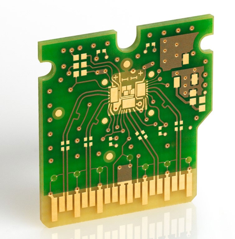
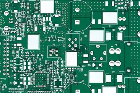
In the harsh environment of space, electronics face intense challenges from radiation that can disrupt or destroy standard printed circuit boards (PCBs). If you're searching for ways to protect spacecraft electronics, the answer lies in radiation hardening techniques. These methods, including specialized PCB design, material selection, and rigorous testing, ensure that electronics can withstand radiation effects like single event effects (SEE) and total ionizing dose (TID). In this comprehensive guide, we'll dive deep into radiation hardened PCB design, rad-hard PCB materials, radiation testing for PCBs, single event effects mitigation, and total ionizing dose (TID) testing to help engineers build reliable systems for space missions.
Why Radiation Hardening Matters for Spacecraft Electronics
Space is an unforgiving environment. High-energy particles from solar flares, cosmic rays, and trapped radiation belts like the Van Allen belts bombard spacecraft electronics relentlessly. Without proper protection, these particles can cause data corruption, system failures, or permanent damage to PCBs. Radiation hardening is the process of designing and building electronics to resist these effects, ensuring mission success for satellites, probes, and crewed spacecraft.
For engineers working on space projects, understanding radiation hardening is critical. It’s not just about preventing failure; it’s about guaranteeing reliability over long missions where repairs are impossible. Let’s explore the core techniques and considerations for creating radiation-hardened PCBs.
Key Radiation Effects on PCBs in Space
Before diving into hardening techniques, it’s important to understand the types of radiation effects that threaten spacecraft electronics:
- Total Ionizing Dose (TID): This is the cumulative damage caused by ionizing radiation over time. It can degrade semiconductor materials, leading to increased leakage currents or threshold voltage shifts in components. TID is often measured in rads or grays, with spacecraft electronics typically needing to withstand doses from 10 krad to over 100 krad depending on mission duration and orbit.
- Single Event Effects (SEE): These are sudden, localized disruptions caused by a single high-energy particle. SEE can result in bit flips (single event upsets or SEU), latch-ups (SEL), or even permanent burnout (SEB) in power transistors. These events are unpredictable and can occur at any time during a mission.
- Displacement Damage: High-energy particles can displace atoms in semiconductor lattices, reducing the performance of components like solar cells and sensors over time.
Understanding these threats is the foundation for effective radiation hardened PCB design. Now, let’s look at practical strategies to mitigate them.
Radiation Hardened PCB Design Techniques
Designing a PCB for space requires a different mindset compared to terrestrial applications. Here are some proven techniques for radiation hardened PCB design:
1. Component Selection and Redundancy
Choosing radiation-tolerant or radiation-hardened components is the first step. These components are specifically engineered to resist TID and SEE. For example, rad-hard microprocessors and memory chips are designed with larger feature sizes (often above 130 nm) to reduce sensitivity to radiation-induced errors, as smaller geometries are more prone to upsets.
Additionally, incorporating redundancy in critical systems can prevent mission failure. Using triple modular redundancy (TMR), where three identical circuits process the same data and vote on the output, helps detect and correct errors caused by SEE. This approach can increase board size and power consumption but is often necessary for critical systems.
2. Circuit Design for Error Mitigation
In single event effects mitigation, circuit design plays a huge role. Error detection and correction (EDAC) codes can be implemented in memory systems to identify and fix bit flips caused by SEU. For instance, Hamming codes can correct single-bit errors and detect double-bit errors, ensuring data integrity.
Another technique is to add guard bands or isolation regions in the PCB layout to prevent latch-up propagation. This involves spacing sensitive components apart and using decoupling capacitors to stabilize power lines, reducing the risk of destructive SEL events.
3. Shielding and Layout Optimization
While shielding cannot stop all radiation, it can reduce the impact of lower-energy particles. Adding thin layers of high-density materials like tantalum or aluminum around sensitive components can help. However, shielding adds weight, which is a critical concern in spacecraft design, so it must be balanced with mission constraints.
In terms of layout, avoid placing high-speed signal traces near power lines or sensitive analog components to minimize noise and interference amplified by radiation effects. Keep trace lengths short to reduce impedance, targeting values below 50 ohms for critical signals, and use ground planes to provide a stable reference and additional shielding.
Rad-Hard PCB Materials: Building for Durability
The choice of materials in PCB manufacturing is just as important as design. Standard materials like FR-4, commonly used in consumer electronics, may degrade under radiation exposure due to outgassing or mechanical breakdown. For space applications, rad-hard PCB materials are essential.
1. Substrate Materials
High-performance materials like polyimide or ceramic-based substrates are preferred for their stability in high-radiation environments. Polyimide offers excellent thermal resistance (up to 300°C) and low outgassing, which prevents contamination in the vacuum of space. Ceramic substrates, while more expensive, provide superior radiation resistance and thermal conductivity, often exceeding 20 W/m·K, making them ideal for high-power applications.
2. Solder and Coatings
Radiation can also affect solder joints, causing embrittlement or cracking over time. Using lead-free solders with high melting points and radiation-resistant properties helps maintain joint integrity. Additionally, conformal coatings made of silicone or parylene can protect PCB surfaces from radiation-induced corrosion and provide an extra barrier against particle impacts.
3. Trace and Via Materials
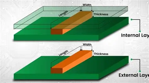
Copper traces are standard, but their thickness and plating must be optimized for radiation environments. Thicker traces (e.g., 2 oz copper or 70 μm) can better withstand current surges caused by SEE. Gold or nickel plating on vias and pads can prevent oxidation and improve reliability under extreme conditions.
Radiation Testing for PCBs: Ensuring Reliability
Designing and building a radiation-hardened PCB is only half the battle. Rigorous radiation testing for PCBs is crucial to validate performance under space-like conditions. Testing identifies weaknesses and ensures the board can survive the mission’s expected radiation levels.
1. Total Ionizing Dose (TID) Testing
Total ionizing dose (TID) testing measures how much cumulative radiation a PCB and its components can endure before performance degrades. This is typically done in a controlled environment using gamma rays from a cobalt-60 source. The test exposes the PCB to incremental doses, often starting at 10 krad and increasing to 100 krad or more, while monitoring parameters like leakage current and threshold voltage shifts in semiconductors.
For example, a typical low Earth orbit (LEO) mission might require electronics to withstand 30 krad over five years, while deep space missions could demand tolerance up to 300 krad. TID testing ensures that the PCB meets or exceeds these thresholds.
2. Single Event Effects (SEE) Testing
SEE testing focuses on the PCB’s response to high-energy particles that cause sudden errors. This is often conducted using heavy ion accelerators to simulate cosmic ray impacts. Engineers measure the rate of single event upsets (SEU) and latch-ups (SEL), aiming for error rates below 1 upset per 10^6 device-hours for critical systems.
Testing also evaluates mitigation strategies like EDAC and TMR. If a memory chip shows a high SEU rate, designers might adjust shielding or switch to a more robust component with a lower cross-section for particle interaction.
3. Environmental and Combined Effects Testing
Beyond radiation, PCBs in space face thermal cycling, vacuum, and vibration. Combined effects testing simulates these conditions alongside radiation exposure to ensure the board performs reliably. For instance, a test might cycle the PCB between -55°C and 125°C while exposing it to 50 krad of TID to mimic a satellite’s orbit through Earth’s shadow and sunlight.
Best Practices for Single Event Effects Mitigation
Single event effects mitigation requires a multi-layered approach. Beyond circuit design and testing, consider these best practices:
- Software Safeguards: Implement watchdog timers in firmware to detect and reset systems after an SEU disrupts operation. This prevents the system from hanging indefinitely.
- Power Management: Use current-limiting circuits to shut down components during a latch-up event, preventing burnout. Target response times under 10 microseconds for optimal protection.
- Component Derating: Operate components below their maximum rated voltage and current (e.g., at 75% of capacity) to reduce stress and improve resilience to radiation-induced failures.
Challenges and Future Trends in Radiation Hardening
While radiation hardening techniques have advanced, challenges remain. The push for smaller, lighter electronics often conflicts with the need for larger, more robust components. Balancing cost, weight, and performance is a constant struggle in spacecraft design.
Looking ahead, innovations like silicon-on-insulator (SOI) technology promise to enhance radiation tolerance by isolating transistors on a thin insulating layer, reducing charge collection from particle strikes. Additionally, machine learning algorithms are being explored to predict and mitigate SEE in real-time, potentially revolutionizing how spacecraft handle radiation events.
Conclusion: Building Reliable Spacecraft Electronics
Radiation hardening is a cornerstone of reliable spacecraft electronics. Through careful radiation hardened PCB design, selection of rad-hard PCB materials, and comprehensive radiation testing for PCBs, engineers can protect systems from the harsh effects of space radiation. Techniques for single event effects mitigation and total ionizing dose (TID) testing ensure that every component performs as expected, even after years in orbit.
At ALLPCB, we understand the unique demands of space applications. Our expertise in high-reliability PCB manufacturing can support your mission with tailored solutions that prioritize durability and performance. Whether you’re designing for low Earth orbit or deep space, mastering radiation hardening is the key to success.
 ALLPCB


