 ALLPCB


In the world of modern electronics, High-Density Interconnect (HDI) PCBs are the backbone of compact, high-performance devices. Whether you're designing for smartphones, medical equipment, or automotive systems, mastering HDI PCB stackup design rules and HDI PCB layer arrangement strategies is critical for ensuring optimal performance. A well-planned stackup not only saves space but also enhances signal integrity and maintains controlled impedance in HDI PCB stackup configurations.
In this comprehensive guide, we’ll walk you through the essentials of HDI PCB stackup design. From understanding the basics to diving into advanced strategies for layer configuration and impedance control, this post will equip you with actionable insights to elevate your PCB projects. Let’s get started!
What Is an HDI PCB Stackup and Why Does It Matter?
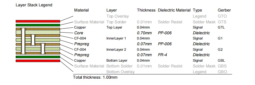
An HDI PCB stackup refers to the arrangement of conductive and insulating layers in a printed circuit board designed for high-density interconnections. Unlike traditional PCBs, HDI boards feature finer lines, smaller vias (like microvias), and denser component placement, often requiring multiple layers to handle complex circuits in a compact footprint.
The stackup design directly impacts signal integrity, power distribution, thermal management, and electromagnetic compatibility (EMC). A poorly configured stackup can lead to signal crosstalk, impedance mismatches, or excessive heat buildup, resulting in device failure. By mastering HDI PCB stackup design rules, engineers can minimize these risks and achieve reliable, high-speed performance.
Key Benefits of Optimized HDI PCB Stackup Design
Before diving into the technical details, let’s explore why investing time in stackup design pays off:
- Improved Signal Integrity: Proper layer arrangement reduces noise and crosstalk, ensuring clean signal transmission, especially at high frequencies (e.g., above 1 GHz).
- Compact Design: HDI stackups allow for more components in less space, ideal for miniaturized devices.
- Better Thermal Management: Strategic placement of ground and power planes helps dissipate heat efficiently.
- Controlled Impedance: Consistent impedance (e.g., 50 ohms for many high-speed signals) is achievable with careful stackup planning, critical for data integrity in high-speed applications.
- Cost Efficiency: Optimized designs reduce material waste and manufacturing errors, lowering production costs.
Fundamental HDI PCB Stackup Design Rules
Designing an HDI PCB stackup requires adherence to specific rules to ensure functionality and manufacturability. Here are the core principles to follow:
1. Define Layer Count Based on Complexity
The number of layers in an HDI PCB depends on the circuit’s complexity. For instance, a simple consumer device might use a 4-layer HDI stackup, while a high-speed networking board could require 8 or more layers. Start by assessing the number of signal nets, power requirements, and component density. As a rule of thumb, allocate at least one ground plane and one power plane to stabilize voltage and minimize noise.
2. Use Symmetrical Stackup for Balance
A symmetrical stackup prevents warping during manufacturing due to uneven thermal expansion. For example, in a 6-layer HDI PCB, place ground and power planes symmetrically (e.g., layers 2 and 5 as ground, layers 3 and 4 as signal). Symmetry also aids in maintaining consistent dielectric thickness, which is crucial for controlled impedance in HDI PCB stackup designs.
3. Minimize Signal Layer Adjacency
Adjacent signal layers can cause crosstalk, especially at high speeds. Always separate signal layers with a ground or power plane to act as a shield. For instance, in an 8-layer stackup, a typical arrangement might be: Signal (Layer 1), Ground (Layer 2), Signal (Layer 3), Power (Layer 4), and so on.
4. Optimize Via Usage
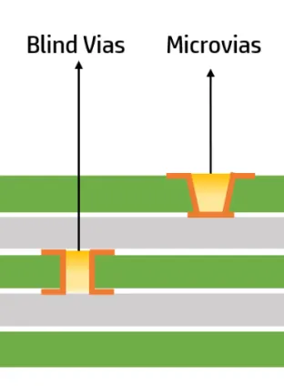
HDI PCBs rely on microvias, blind vias, and buried vias for inter-layer connections. Use microvias (typically 0.1 mm in diameter) for high-density areas to save space, but limit their depth to 1-2 layers to maintain reliability. Avoid stacking vias directly on top of each other to prevent stress points during fabrication.
HDI PCB Layer Arrangement Strategies for Optimal Performance
Effective HDI PCB layer arrangement strategies are the cornerstone of high-performing boards. Below are proven approaches to configure layers for maximum efficiency:
1. Prioritize Ground Planes for Signal Integrity
Ground planes are essential for providing a low-impedance return path for signals, reducing electromagnetic interference (EMI). Place a ground plane adjacent to every signal layer, especially for high-speed signals above 500 MHz. For example, in a 4-layer HDI PCB, a common stackup might be: Signal (Top), Ground, Power, Signal (Bottom).
2. Group Power Planes for Efficient Distribution
Power planes should be placed centrally in the stackup to distribute voltage evenly across the board. If multiple voltage levels are needed (e.g., 3.3V and 5V), split the power plane into sections or use multiple power layers, ensuring each is paired with a nearby ground plane to minimize loop inductance.
3. Allocate Signal Layers for Routing Density
In HDI designs, signal layers handle dense routing with fine traces (often 3-5 mils wide). Dedicate outer layers for high-speed signals to minimize via transitions, which can introduce signal delays. Inner signal layers can handle slower signals or less critical nets. Keep trace lengths short (under 1 inch for signals above 1 GHz) to avoid signal degradation.
4. Incorporate Dielectric Thickness for Impedance Control
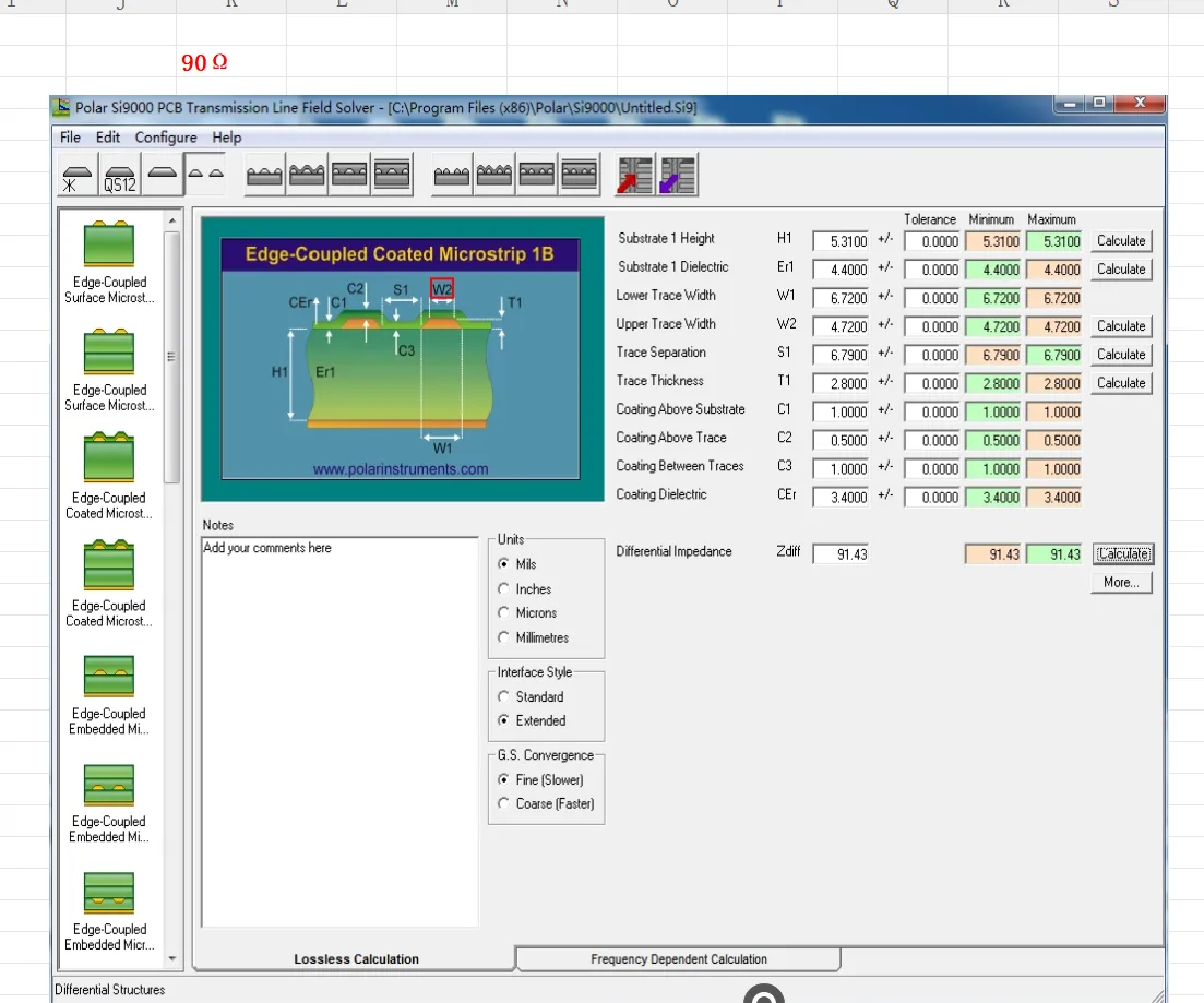
The dielectric material and its thickness between layers directly affect impedance. For controlled impedance in HDI PCB stackup, maintain uniform dielectric thickness (e.g., 4 mils for a 50-ohm trace) and choose materials with stable dielectric constants (Dk), such as FR-4 (Dk ≈ 4.2) or high-frequency laminates (Dk ≈ 3.0-3.5). Use impedance calculators or simulation tools to verify values during design.
Controlled Impedance in HDI PCB Stackup: A Deeper Dive
Controlled impedance is a critical aspect of HDI PCB design, especially for high-speed applications like USB 3.0, HDMI, or DDR memory interfaces. Impedance mismatches can cause signal reflections, leading to data errors or system crashes. Here’s how to achieve controlled impedance in HDI PCB stackup:
1. Calculate Trace Geometry Precisely
Impedance depends on trace width, thickness, and the dielectric material surrounding it. For a 50-ohm single-ended trace on a standard FR-4 substrate, a trace width of 6 mils with a dielectric height of 4 mils is often ideal. Use simulation software to fine-tune these parameters based on your stackup.
2. Maintain Consistent Layer Spacing
Variations in dielectric thickness can alter impedance. Ensure manufacturing tolerances are tight (e.g., ±10% for dielectric height) to avoid deviations. For differential pairs (common in high-speed designs), keep spacing between traces consistent (e.g., 5 mils apart for 100-ohm differential impedance).
3. Test and Validate Impedance Post-Manufacturing
After fabrication, use a Time Domain Reflectometer (TDR) to measure impedance across critical traces. If values deviate (e.g., reading 55 ohms instead of 50 ohms), adjust trace widths or dielectric materials in future revisions. Most HDI designs target a tolerance of ±5% for impedance-critical nets.
Common Challenges in HDI PCB Stackup Design and How to Overcome Them
Even with careful planning, HDI stackup design can present hurdles. Here are common issues and solutions:
- Signal Crosstalk: Caused by closely spaced traces or adjacent signal layers. Solution: Increase spacing (at least 3x trace width) or add ground shielding between layers.
- Thermal Hotspots: High-density components generate heat. Solution: Use thermal vias and place power planes near heat sources to spread heat evenly.
- Manufacturing Constraints: Fine features like microvias can be hard to fabricate. Solution: Collaborate with your manufacturer early to align design rules (e.g., minimum via size of 0.1 mm) with their capabilities.
Advanced Tips for HDI PCB Stackup Optimization
For engineers looking to push the boundaries of HDI design, consider these advanced strategies:
- Use Build-Up Technology: Sequential build-up (SBU) processes allow for additional HDI layers with microvias, enabling ultra-dense designs.
- Adopt High-Frequency Materials: For signals above 5 GHz, use low-loss materials with a dissipation factor (Df) below 0.005 to minimize signal attenuation.
- Simulate Before Fabrication: Leverage electromagnetic simulation tools to model signal behavior and impedance across the stackup, catching issues before production.
Conclusion: Build Better HDI PCBs with Strategic Stackup Design
Mastering HDI PCB stackup design rules and HDI PCB layer arrangement strategies is a game-changer for engineers working on compact, high-performance electronics. By prioritizing symmetry, signal integrity, and controlled impedance in HDI PCB stackup, you can create boards that meet the stringent demands of modern applications. From selecting the right number of layers to fine-tuning dielectric thickness, every decision in stackup design plays a role in the final product’s success.
Start applying these principles in your next project to achieve reliable, efficient, and cost-effective HDI PCBs. With careful planning and attention to detail, you’ll be well on your way to designing boards that stand out in performance and durability.


