ALLPCB


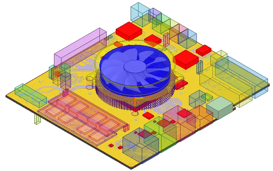
Designing high-performance Electronic Control Unit (ECU) PCBs requires careful attention to component placement. Optimizing PCB layout is a critical step in ensuring signal integrity, thermal management, and overall system reliability in automotive applications. In this comprehensive guide, we’ll explore effective strategies for component placement, ECU PCB design, and optimizing PCB layout to achieve a high-performance PCB. Whether you’re an engineer or a designer, you’ll find actionable tips and insights to enhance your PCB design strategy.
Why Component Placement Matters in ECU PCB Design
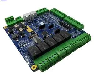
In ECU PCB design, component placement directly impacts the performance, reliability, and manufacturability of the board. ECUs are the brain of modern vehicles, controlling everything from engine performance to safety systems. A poorly optimized layout can lead to issues like signal interference, overheating, or even system failure. By focusing on strategic component placement, you can minimize these risks and ensure the ECU operates efficiently under demanding conditions.
Proper placement reduces signal delays, lowers electromagnetic interference (EMI), and improves thermal dissipation. For instance, placing high-speed components closer to their corresponding connectors can reduce signal propagation delays by up to 20%, depending on the trace length and board material. Let’s dive into the key principles and strategies for achieving an optimized layout for high-performance PCBs.
Key Principles of Component Placement for High-Performance PCBs
Before starting the layout process, it’s essential to understand the foundational principles of component placement in ECU PCB design. These guidelines help ensure that your board meets performance and reliability standards.
1. Prioritize Functional Grouping
Group components based on their function to minimize trace lengths and improve signal integrity. For example, place microcontrollers, memory chips, and related peripherals close together to reduce latency in data transfer. In an ECU, the power management section should be isolated from sensitive analog circuits to prevent noise coupling. This approach can reduce crosstalk by as much as 15% in high-speed designs.
2. Minimize Signal Path Lengths
Shorter signal paths mean faster transmission and less chance of interference. For high-speed signals in ECUs, such as CAN bus or Ethernet communications, keep traces under 50 mm where possible to maintain signal integrity. Position critical components like oscillators near the microcontroller to avoid delays, as even a 10 mm increase in trace length can introduce noticeable timing issues at frequencies above 100 MHz.
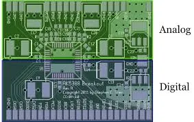
3. Isolate Analog and Digital Sections
In ECU designs, analog and digital circuits often coexist. Mixing these can lead to noise issues, especially in sensor interfaces. Place analog components, like amplifiers or ADCs, away from digital switching elements like processors. Use ground planes to create barriers, reducing noise by up to 30% in mixed-signal designs.
4. Consider Thermal Management
ECUs often operate in harsh environments with high temperatures. Place heat-generating components, such as power regulators or MOSFETs, near the board’s edges or heat sinks to dissipate heat effectively. Ensure a clearance of at least 5 mm around high-power components to prevent thermal hotspots, which can reduce component lifespan by 50% if not managed properly.
Step-by-Step PCB Design Strategy for Optimizing Layout
With the principles in mind, let’s walk through a structured approach to optimizing PCB layout for a high-performance ECU. This step-by-step PCB design strategy ensures that every aspect of component placement is addressed systematically.
Step 1: Define Design Constraints and Requirements
Start by identifying the electrical, mechanical, and thermal constraints of your ECU. For example, determine the maximum current draw (e.g., 5A for power circuits) and voltage levels (e.g., 12V or 48V for automotive systems). Also, consider the physical size of the enclosure and any environmental factors, such as operating temperatures ranging from -40°C to 85°C. These constraints will guide your placement decisions.
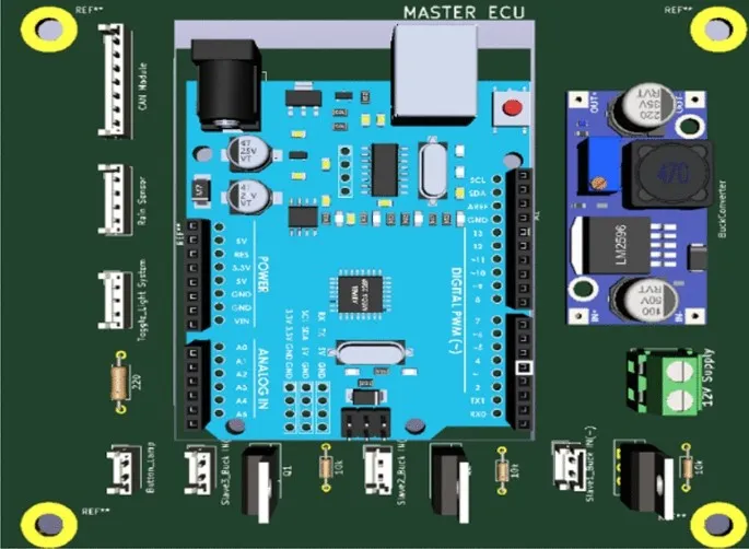
Step 2: Create a Preliminary Floorplan
Sketch a rough floorplan of the PCB, allocating space for major functional blocks like power supply, processing unit, and communication interfaces. Place connectors and fixed components first, as their positions are often dictated by mechanical requirements. For instance, a CAN bus connector might need to be at the board’s edge for easy access, influencing the placement of related ICs.
Step 3: Place Critical Components
Position high-priority components such as microcontrollers, clocks, and high-speed transceivers early in the process. These components often dictate the routing of critical signals. For example, placing a crystal oscillator within 10 mm of the microcontroller minimizes parasitic capacitance, ensuring stable clock signals at frequencies like 16 MHz or higher.
Step 4: Route Power and Ground Planes
Before placing secondary components, establish robust power and ground planes. In ECU designs, a solid ground plane reduces impedance and EMI, often lowering noise levels by 10-20 dB compared to split planes. Place decoupling capacitors (e.g., 0.1 μF ceramics) within 3 mm of IC power pins to stabilize voltage and filter noise, especially for high-frequency operations above 50 MHz.
Step 5: Optimize Remaining Component Placement
With critical components and power planes in place, position the remaining parts. Keep signal paths short and direct, avoiding unnecessary vias that increase resistance. For instance, in an ECU handling sensor data, place analog-to-digital converters near sensor inputs to keep analog traces under 25 mm, reducing noise pickup.
Step 6: Verify Clearances and Design Rules
Ensure adequate spacing between components to prevent interference and ease manufacturing. Maintain a minimum clearance of 0.5 mm between components and 0.25 mm between traces for standard designs. For high-voltage sections in hybrid or electric vehicle ECUs, increase clearance to 2 mm or more to prevent arcing at voltages above 48V.
Advanced Tips for High-Performance PCB Layout Optimization
Beyond the basics, there are advanced techniques that can further enhance the performance of your ECU PCB. These strategies focus on fine-tuning your design for maximum efficiency and reliability.
1. Use Simulation Tools for Validation
Before finalizing your layout, use simulation software to analyze signal integrity and thermal performance. Tools can predict potential issues like signal reflections or hot spots. For instance, simulations might show that a trace impedance of 50 ohms is ideal for high-speed CAN signals, allowing you to adjust trace widths (e.g., 0.2 mm for FR-4 material) accordingly.
2. Optimize for EMI Reduction
EMI is a major concern in automotive environments. Place components to minimize loop areas in high-current paths, as larger loops act as antennas for EMI. For example, positioning a switching regulator’s input and output capacitors within 2 mm of each other can reduce loop inductance by 40%, cutting EMI significantly.
3. Account for Manufacturing Tolerances
Design with manufacturing in mind to avoid costly rework. Ensure component footprints match the assembly process, and leave at least 1 mm of space around fine-pitch components (e.g., 0.5 mm pitch QFN packages) for soldering accuracy. This reduces the risk of defects by up to 25% during production.
4. Plan for Scalability and Updates
ECU designs often evolve with new features or standards. Leave extra space near key components like microcontrollers for potential upgrades or additional circuitry. For instance, reserving 10% of board area for future expansion can save redesign costs if a new sensor interface is added later.
Common Mistakes to Avoid in ECU PCB Component Placement
Even experienced designers can make errors in component placement that compromise performance. Here are some pitfalls to watch out for in your high-performance PCB layout.
Overcrowding Components: Packing components too closely can lead to thermal and interference issues. Maintain at least 3 mm spacing around high-power parts to allow heat dissipation and ease assembly.
Ignoring Signal Return Paths: Failing to consider return paths for high-speed signals can cause EMI. Always route return paths directly under signal traces on a continuous ground plane to minimize loop area, reducing impedance by up to 30%.
Neglecting Mechanical Constraints: Components placed without considering the enclosure or mounting points may lead to assembly issues. For example, tall components near connectors might interfere with housing, requiring a redesign.
Poor Decoupling Capacitor Placement: Placing decoupling capacitors too far from ICs can render them ineffective. Keep them within 3 mm of power pins to ensure a stable supply, especially for ICs operating at 3.3V or lower.
Conclusion: Building Better ECUs with Optimized Component Placement
Optimizing component placement is a cornerstone of ECU PCB design and a vital part of creating a high-performance PCB. By following a structured PCB design strategy and applying the tips shared in this guide, you can enhance signal integrity, manage heat effectively, and reduce EMI in your designs. From grouping components logically to using simulation tools for validation, every step in optimizing PCB layout contributes to a more reliable and efficient ECU.
Start with a clear plan, prioritize critical components, and always keep manufacturing and environmental factors in mind. With these practices, your ECU PCBs will not only meet but exceed performance expectations in the demanding automotive industry. Focus on precision in component placement, and you’ll build boards that power vehicles with unmatched reliability.