 ALLPCB


In the world of electronics, printed circuit boards (PCBs) are often thought of as rigid, rectangular components that follow strict design rules. But what if you could break free from these constraints and explore unconventional PCB design with non-rectangular PCB shapes and irregular PCB shapes? At ALLPCB, we believe that creativity and innovation in advanced PCB manufacturing techniques can lead to groundbreaking designs, especially when working with minimum PCB sizes. This blog dives deep into how you can push the boundaries with creative PCB layouts to achieve unique, efficient, and high-performing designs.
Whether you're an engineer looking to optimize space in a compact device or a designer aiming to create a visually striking product, unconventional PCB designs can open up new possibilities. Let’s explore the benefits, challenges, and practical tips for designing PCBs that defy traditional norms.
Why Consider Unconventional PCB Designs?
Traditional PCB designs often stick to rectangular shapes due to ease of manufacturing and assembly. However, as devices become smaller and more complex, sticking to these norms can limit innovation. Unconventional PCB design offers several advantages, especially when dealing with minimum PCB sizes:
- Space Optimization: Non-rectangular and irregular shapes allow PCBs to fit into tight or uniquely shaped enclosures, maximizing the use of available space in devices like wearables or IoT gadgets.
- Enhanced Aesthetics: For consumer products, a creative PCB layout can serve as a visual feature, adding a unique look to the product.
- Improved Functionality: Irregular shapes can help with signal routing, heat dissipation, or component placement in ways that standard designs cannot.
By adopting advanced PCB manufacturing techniques, designers can create boards as small as 5mm x 5mm while maintaining high performance, pushing the boundaries of what’s possible.
Exploring Non-Rectangular and Irregular PCB Shapes
When we talk about non-rectangular PCB and irregular PCB shapes, we mean designs that deviate from the typical square or rectangular form. These can include circular, triangular, or custom shapes with cutouts, slots, or curves. Here’s why and how these shapes are becoming more popular:
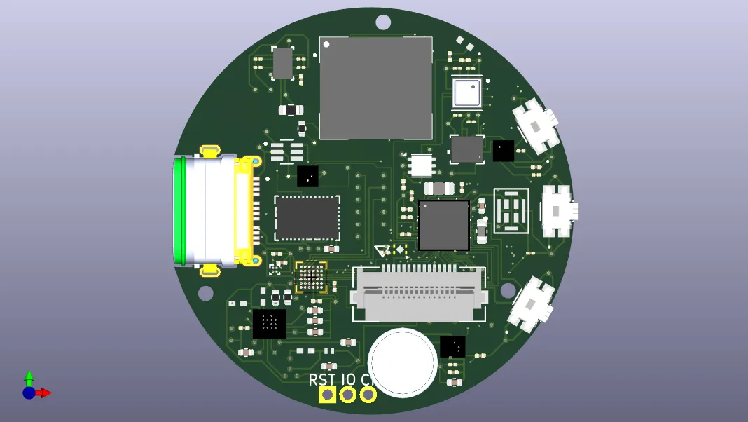
1. Circular PCBs for Compact Devices
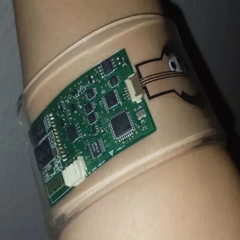
Circular PCBs are often used in devices like smartwatches or sensors where a round enclosure is necessary. These boards can reduce wasted space and align better with the device’s external design. For instance, a circular PCB with a diameter as small as 10mm can house essential components for a basic sensor module, maintaining signal integrity with proper trace routing.
2. Triangular or Polygonal Shapes for Unique Applications
Triangular or polygonal PCBs are less common but can be ideal for specific applications, such as fitting into corner spaces of a larger assembly or creating modular designs. These shapes can also help with thermal management by distributing heat more evenly across non-standard geometries.
3. Custom Shapes with Cutouts and Slots
Custom PCBs with cutouts and slots allow for precise fitting around other components or enclosures. For example, a PCB with a central cutout can accommodate a battery or a display module, reducing the overall footprint. However, these designs require careful planning to avoid stress points that could lead to board cracking during assembly or use.
Challenges of Designing Unconventional Minimum PCB Sizes
While the benefits of unconventional PCB design are clear, working with minimum PCB sizes and irregular shapes comes with unique challenges. Understanding these hurdles can help you plan better and achieve successful outcomes using advanced PCB manufacturing techniques.
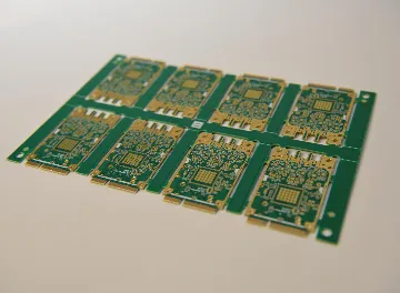
1. Manufacturing Complexity
Non-standard shapes often require specialized tooling and processes, which can increase production time and cost. For instance, routing traces on a board smaller than 10mm x 10mm demands high precision to avoid signal interference or crosstalk, especially at high frequencies above 1 GHz.
2. Component Placement and Routing
Irregular shapes can limit the space available for components and traces. Designers must carefully plan the layout to ensure that critical signals maintain impedance values, such as 50 ohms for RF applications, while avoiding sharp corners that could cause signal reflection.
3. Mechanical Stress and Durability
Non-rectangular designs, especially those with cutouts, are more prone to mechanical stress. During manufacturing or operation, areas with sharp angles or thin sections can crack if not reinforced properly. Using materials with a higher tensile strength or adding support structures can mitigate this risk.
Advanced PCB Manufacturing Techniques for Unconventional Designs
To successfully bring creative PCB layouts to life, leveraging advanced PCB manufacturing techniques is essential. Here are some cutting-edge methods that make unconventional designs possible, even at minimum PCB sizes:
1. High-Density Interconnect (HDI) Technology
HDI technology allows for finer traces and smaller vias, enabling designers to pack more functionality into tiny boards. For example, microvias with diameters as small as 0.1mm can be used on boards smaller than 8mm x 8mm, supporting complex layouts without sacrificing performance.
2. Laser Cutting for Precision Shapes
Laser cutting is often used to create precise irregular PCB shapes. This method ensures clean edges and accurate dimensions, even for intricate designs with curves or slots. It’s particularly useful for prototypes or small-batch production where customization is key.
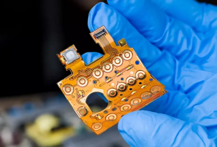
3. Flexible and Rigid-Flex PCBs
Flexible and rigid-flex PCBs can be shaped into non-standard forms, making them ideal for unconventional designs. These materials allow the board to bend or fold into unique configurations, fitting into spaces where rigid boards cannot. For instance, a flexible PCB with a minimum width of 3mm can wrap around a cylindrical enclosure for a medical device.
Tips for Designing Creative PCB Layouts with Minimum Sizes
Designing creative PCB layouts with unconventional shapes and minimum sizes requires a strategic approach. Here are some actionable tips to guide you through the process:
1. Start with a Clear Purpose
Define why you need an unconventional shape. Is it to fit a specific enclosure, improve signal flow, or enhance aesthetics? Having a clear goal will guide your design decisions and prevent unnecessary complexity.
2. Use Simulation Tools for Validation
Before manufacturing, use simulation software to test signal integrity, thermal performance, and mechanical stress. For example, ensure that high-speed signals maintain a consistent impedance of 50 ohms across irregular trace paths to avoid data loss or interference.
3. Optimize Component Placement
Prioritize critical components first, placing them in areas with the most space or best thermal dissipation. For tiny boards under 10mm x 10mm, consider using surface-mount components with smaller footprints, like 0402 or 0201 packages, to save space.
4. Collaborate with Your Manufacturer Early
Work closely with your manufacturing partner to understand their capabilities and limitations for non-rectangular PCB designs. Discuss minimum trace widths (often as low as 3 mils for advanced processes) and spacing to ensure your design is feasible for production.
Real-World Applications of Unconventional PCB Designs
Unconventional PCB designs are not just theoretical—they’re already making an impact in various industries. Here are a few examples of how irregular PCB shapes and minimum sizes are being used:
- Wearable Technology: Smartwatches and fitness trackers often use circular or curved PCBs to fit snugly within small, ergonomic designs. These boards, sometimes as small as 7mm in diameter, support complex circuits for sensors and wireless communication.
- Automotive Systems: In vehicles, PCBs with custom cutouts are used to fit around other components, optimizing space in crowded dashboards or engine control units.
- Medical Devices: Tiny, flexible PCBs with non-standard shapes are critical for implantable devices, ensuring they conform to the body’s contours while maintaining reliable performance.
Conclusion: Embrace the Future with Unconventional PCB Designs
Breaking away from traditional rectangular designs and embracing unconventional PCB design can unlock new levels of innovation, especially when working with minimum PCB sizes. By exploring non-rectangular PCB forms, irregular PCB shapes, and creative PCB layouts, you can create products that stand out in both form and function. With the support of advanced PCB manufacturing techniques from ALLPCB, the possibilities are endless.
Whether you’re designing for a compact wearable, a unique consumer product, or a high-performance industrial application, don’t be afraid to think outside the box. Unconventional designs may come with challenges, but the rewards of optimized space, enhanced aesthetics, and improved functionality are well worth the effort. Start experimenting with your next project, and let your creativity shape the future of electronics.


