 ALLPCB


In the world of electronics design, not every project fits neatly into a standard rectangular box. When faced with odd-shaped enclosures, creating a PCB that fits perfectly while maintaining functionality can be a challenge. How do you design PCBs for irregular shapes or custom outlines? The answer lies in understanding irregular PCB shapes, mastering custom PCB outlines, and navigating the unique PCB design constraints that come with odd-shaped enclosures. In this blog, we’ll dive deep into the process of designing creative PCB layouts to ensure your board fits seamlessly into any enclosure, no matter how unconventional.
Whether you’re working on a wearable device, a compact IoT gadget, or a specialized industrial tool, this guide will walk you through practical steps, design tips, and key considerations to achieve a perfect fit. Let’s explore how to go beyond the box and create PCBs tailored for unique designs.
Why Odd-Shaped Enclosures Matter in PCB Design
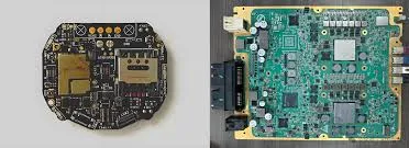
Odd-shaped enclosures are often a necessity in modern electronics. Think about smartwatches with curved edges, automotive sensors squeezed into tight spaces, or drones with aerodynamic designs. These products demand PCBs that conform to specific shapes rather than standard rectangles or squares. Designing for such enclosures isn’t just about aesthetics—it’s about optimizing space, ensuring functionality, and meeting the physical constraints of the product.
Irregular PCB shapes allow engineers to maximize the use of limited space, reduce material waste, and improve the overall design of a device. However, these designs come with unique challenges, such as maintaining signal integrity, managing heat dissipation, and ensuring manufacturability. By addressing these challenges early in the design phase, you can create a board that fits perfectly while performing reliably.
Key Challenges of Designing for Irregular PCB Shapes
Before diving into the design process, it’s important to understand the hurdles that come with irregular PCB shapes and odd-shaped enclosures. Here are some of the most common PCB design constraints you’ll encounter:
- Space Limitations: Odd-shaped enclosures often have tight corners, curves, or cutouts that restrict where components can be placed. This can make routing traces more complex.
- Signal Integrity: Non-standard shapes can lead to uneven trace lengths, increasing the risk of signal delays or interference. For high-speed designs, this can result in impedance mismatches, with values deviating from the ideal 50 ohms commonly targeted for controlled impedance lines.
- Thermal Management: Irregular shapes may disrupt airflow or heat dissipation patterns, leading to hotspots on the board. Without proper planning, critical components could overheat.
- Manufacturing Constraints: Not all fabrication processes are suited for custom PCB outlines. Cutting complex shapes or adding slots and cutouts can increase costs and lead times.
- Mechanical Stress: Unusual shapes can create stress points during assembly or use, risking cracks or board failure if not reinforced properly.
Understanding these challenges helps set realistic expectations and guides the design process. Let’s now look at how to tackle them with practical solutions and creative PCB layouts.
Steps to Design PCBs for Odd-Shaped Enclosures
Designing a PCB for an odd-shaped enclosure requires a systematic approach. Follow these steps to ensure your board fits perfectly while meeting performance and manufacturing needs.
1. Start with the Enclosure Design
The first step is to fully understand the enclosure’s dimensions and shape. Use 3D modeling tools to visualize how the PCB will fit inside the enclosure. Many design software platforms allow for ECAD (Electronic Computer-Aided Design) and MCAD (Mechanical Computer-Aided Design) co-design, letting you import the enclosure’s 3D model directly into your PCB layout environment. This helps identify potential clearance issues or areas where the board outline needs to be adjusted.
Ensure there’s enough space for mounting holes, connectors, and any protrusions like buttons or displays. A clearance of at least 1-2 mm between the PCB edge and enclosure walls is often recommended to account for manufacturing tolerances and assembly ease.
2. Define a Custom PCB Outline
Once you have the enclosure model, define the custom PCB outline to match the shape. Most PCB design tools allow you to draw irregular shapes by specifying coordinates or importing a DXF file of the enclosure’s internal dimensions. Be precise—errors in the outline can lead to a board that doesn’t fit or requires costly revisions.
For complex shapes, consider breaking the design into smaller sections or using cutouts to accommodate enclosure features. Keep in mind that sharp corners in the PCB outline can create stress points, so aim for rounded edges where possible, with a minimum radius of 0.5 mm to ease manufacturing.
3. Optimize Component Placement for Irregular PCB Shapes
With an irregular shape, component placement becomes trickier. Place critical components first, such as microcontrollers, power regulators, and connectors, ensuring they align with enclosure openings or mounting points. Group related components together to minimize trace lengths, especially for high-speed signals where delays can impact performance. For instance, in a design with a 100 MHz clock signal, keeping trace lengths under 30 mm can help avoid timing issues.
Use the enclosure’s shape to your advantage. If there are curved areas, place smaller components like resistors or capacitors there, reserving flat or central areas for larger components like ICs or heat sinks.
4. Route Traces with Care
Routing traces on an irregular PCB shape requires extra attention. Avoid running traces near the board’s edge to prevent damage during manufacturing or assembly—maintain a keep-out zone of at least 0.5 mm from the edge. For high-speed designs, ensure consistent trace widths (e.g., 0.2 mm for a 50-ohm impedance line) and avoid sharp bends, using 45-degree angles instead to reduce signal reflection.
If the shape forces long or uneven trace lengths, consider differential pair routing or adding delay-matching techniques to maintain signal integrity. Simulation tools can help verify that signal speeds and timing meet design requirements.
5. Address Thermal and Mechanical Concerns
Odd-shaped enclosures can limit airflow, so plan for thermal management early. Add thermal vias under heat-generating components like power ICs, targeting a via density of 8-10 vias per square centimeter for effective heat transfer to a ground plane. If the enclosure allows, include mounting points for heat sinks or fans.
Mechanically, reinforce weak areas of the PCB, such as narrow sections or cutouts, by increasing the board thickness (e.g., from 1.6 mm to 2.0 mm) or adding support structures in the enclosure design. This reduces the risk of cracking during handling or vibration.
6. Verify Manufacturability
Not all manufacturers can handle complex custom PCB outlines without additional costs or delays. Before finalizing your design, check with your fabrication partner to confirm their capabilities for irregular PCB shapes. Common constraints include minimum slot widths (typically 0.8 mm) and maximum panel utilization, which affects cost. Request a design rule check (DRC) to ensure the outline and features comply with manufacturing tolerances, often within ±0.1 mm for board dimensions.
Also, consider the assembly process. Odd shapes may require custom jigs or fixtures for soldering and testing, so plan for these in advance to avoid production bottlenecks.
Creative PCB Layouts: Thinking Outside the Box
Designing for odd-shaped enclosures isn’t just about overcoming constraints—it’s also an opportunity to get creative with your PCB layouts. Here are some innovative ideas to inspire your next project:
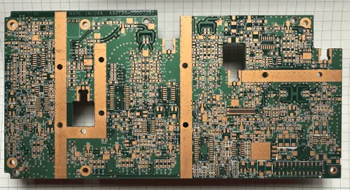
- Multi-Board Designs: If a single irregular PCB shape is too complex or costly to manufacture, split the design into multiple smaller boards connected by flex cables or connectors. This approach works well for enclosures with multiple compartments or levels.
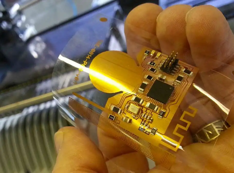
- Flexible PCBs: For enclosures with extreme curves or bends, consider using flexible PCBs that can conform to the shape. These are ideal for wearables or compact devices, though they require careful planning for layer stack-up and bend radius (typically a minimum of 6 times the board thickness).
- Modular Cutouts: Design the PCB with modular cutouts or perforations that allow it to be adapted to different enclosure shapes during assembly. This adds versatility to the board for future iterations or product variations.
- Aesthetic Integration: Use the PCB’s shape as a design element. For consumer products, an exposed PCB with a unique outline can enhance visual appeal, especially if paired with creative silkscreen artwork or LED placements.
Tools and Resources for Designing Custom PCB Outlines
Modern design software makes it easier than ever to create custom PCB outlines for odd-shaped enclosures. Many tools offer features like 3D visualization, design rule checks, and direct integration with mechanical models. Look for software that supports DXF or STEP file imports to streamline the process of matching your PCB to the enclosure.
Additionally, online resources and communities can provide valuable insights into overcoming PCB design constraints. Forums and tutorials often share real-world examples of irregular PCB shapes, offering tips on everything from trace routing to thermal management.
Best Practices for Success with Odd-Shaped Enclosures
To wrap up, here are some best practices to ensure your PCB design for an odd-shaped enclosure is a success:
- Collaborate early with mechanical engineers to align the PCB and enclosure designs, minimizing surprises during assembly.
- Simulate your design for signal integrity and thermal performance before fabrication, using tools that can model real-world conditions.
- Start with a prototype to test the fit and functionality of your custom PCB outline in the actual enclosure. Even small errors (e.g., a 0.2 mm mismatch) can cause issues.
- Document every step of the design process, including enclosure dimensions, keep-out zones, and manufacturing notes, to simplify future revisions or troubleshooting.
Conclusion: Embrace the Challenge of Irregular PCB Shapes
Designing PCBs to fit odd-shaped enclosures is no small task, but it’s a rewarding challenge that pushes the boundaries of creativity and engineering. By carefully planning your custom PCB outline, addressing PCB design constraints, and exploring creative PCB layouts, you can create boards that not only fit perfectly but also enhance the overall performance and appeal of your product.
At ALLPCB, we’re committed to supporting engineers in bringing their innovative designs to life, no matter how unconventional the shape. With the right approach and tools, you can go beyond the box and turn even the most complex enclosures into opportunities for standout designs. Start experimenting with irregular PCB shapes today, and see how far your creativity can take you.


